Tunable micro-bolometer image element structure and image element array

A technology of microbolometer and pixel structure, applied in optical radiation measurement, electric radiation detector, radiation pyrometry, etc., can solve the problem of high electrostatic driving voltage and limitation of Fabry-Perot resonant cavity parallelism and other issues, to achieve the effect of improving parallelism, narrowing absorption bandwidth, and reducing electrostatic driving voltage

Active Publication Date: 2016-07-06
YANTAI RAYTRON TECH
6 Cites 19 Cited by

AI-Extracted Technical Summary

Problems solved by technology

[0005] The existing technology mainly has the following deficiencies: 1. High electrostatic driving voltage is r...

Abstract

The invention relates to a tunable micro-bolometer image element structure comprising a substrate, a bottom electrode, a reflection layer and an absorption layer. The bottom electrode is fixedly arranged at the upper end surface of the substrate. The substrate is provided with stand columns which are fixedly provided with a first supporting device. The absorption layer is fixedly connected with the first supporting device and arranged above the bottom electrode. The upper end of the absorption layer is fixedly provided with heat-sensitive material. The reflection layer is arranged between the bottom electrode and the absorption layer. The reflection layer is connected with the stand columns through a movable second supporting device. A Fabry-Perot resonator is formed between the reflection layer and the absorption layer. Reference potential is accessed to the reflection layer. Electrostatic driving voltage is accessed to the bottom electrode. Electrostatic force is formed between the reflection layer and the bottom electrode to push the reflection layer to longitudinally move. Compared with the structures in the prior art, depth of parallelism of the Fabry-Perot resonator can be improved, absorption bandwidth can be narrowed, absorption rate can be enhanced and electrostatic driving voltage can be reduced.

Application Domain

Pyrometry using electric radation detectors

Technology Topic

Absorption rateAbsorption bandwidth +7

Image

  • Tunable micro-bolometer image element structure and image element array
  • Tunable micro-bolometer image element structure and image element array
  • Tunable micro-bolometer image element structure and image element array

Examples

  • Experimental program(1)

Example Embodiment

[0021] The principles and features of the present invention will be described below with reference to the accompanying drawings. The examples cited are only used to explain the present invention, and are not used to limit the scope of the present invention.
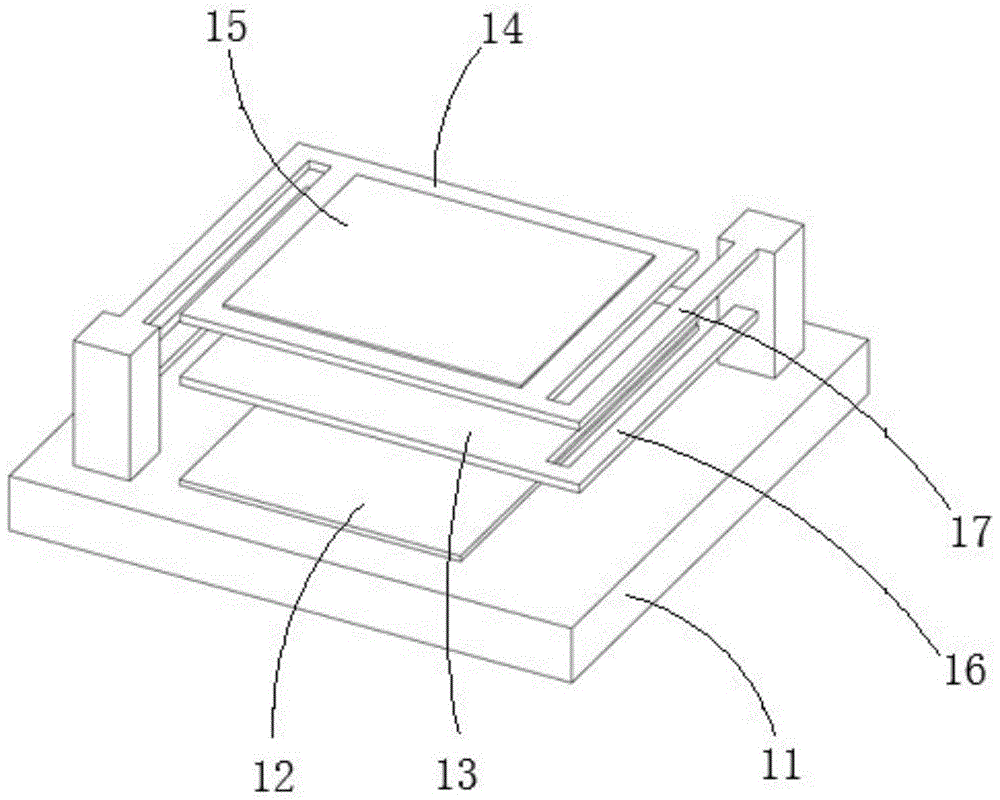
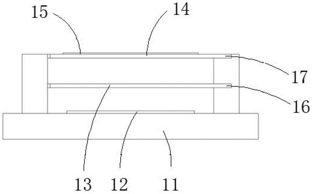
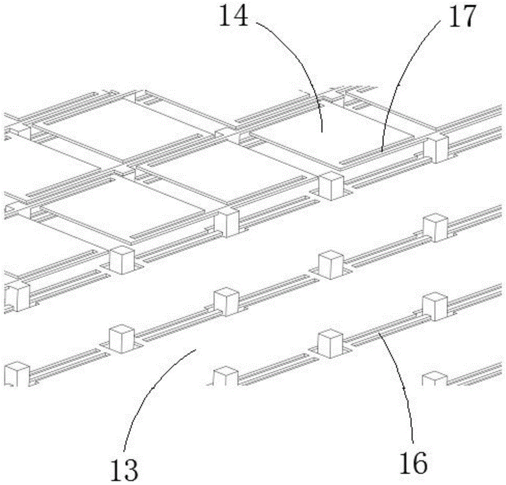
[0022] Such as figure 1 with figure 2 As shown, a tunable microbolometer pixel structure includes a substrate 11, a bottom electrode 12, a reflective layer 13, and an absorption layer 14. The bottom electrode 12 is fixed on the upper end surface of the substrate 11 , A column is provided on the substrate 11, a first supporting device 17 is fixedly provided on the column, and the absorption layer 14 is fixedly connected to the first supporting device 17 and is located above the bottom electrode 12 The upper end of the absorption layer 14 is fixedly provided with a heat-sensitive material 15; the reflection layer 13 is placed between the bottom electrode 12 and the absorption layer 14, and the reflection layer 13 is connected to each other through a movable second supporting device 16 The columns are connected, the reflective layer 13 and the absorption layer 14 form a Fabry-Perot resonant cavity; the reflective layer 13 is connected to a reference potential, and the bottom electrode 12 is connected to an electrostatic driving voltage, so The electrostatic force formed between the reflective layer 13 and the bottom electrode 12 pushes the reflective layer 13 to move longitudinally.
[0023] Preferably, the thermosensitive material absorbs and converts infrared radiation energy.
[0024] Preferably, a plurality of said pixel structures are arranged to form a pixel array structure.
[0025] In the implementation of this device, there is a potential gradient distribution on the absorption layer 14, and the potential difference between the absorption layer 14 and the reflection layer 13 is very small, so that the electrostatic force difference at different positions between the absorption layer 14 and the reflection layer 13 is minimized, The electrostatic force is proportional to the square of the potential difference, that is, F=kV 2 Taking 0V and 2V at both ends of the absorption layer 14 as an example, the reflection layer 13 is connected to the reference potential 0V, while the potential of the traditional structure reflection layer is 10V. If other conditions are the same, the maximum electrostatic force difference between the two ends of the absorption layer 14 is 4k. It is smaller than 36k of the traditional structure, and the absorption layer 14 is connected to the first support device 17, and its elastic coefficient is larger than that of the traditional structure, so the parallelism between the absorption layer 14 and the substrate 11 can be improved compared with the traditional structure.
[0026] Such as image 3 As shown, a tunable microbolometer pixel array includes a pixel structure, the pixel structure is provided with multiple, and the reflective layers 13 of the multiple pixel structures share one or more second supports The device 16 forms a multi-support structure in the plane of the reflective layer 13.
[0027] The present invention also has better control of the parallelism between the reflective layer 13 and the substrate 11, and the difference in electrostatic force between the reflective layer 13 and the absorption layer 14 at different positions is very small; at the same time, the reflective layer 13 and the bottom electrode 12 The voltage difference at all positions is the same, and the electrostatic force difference between them is zero at different positions; in the traditional structure of the Fabry-Perot cavity, the second supporting device 16 is distributed around the reflective layer, and In this structure, the second supporting device 16 of the reflective layer 13 can adopt multiple second supporting devices 16 in the plane of the reflective layer 13, and the design of multiple second supporting devices 16 can maintain the parallelism of the reflective layer 13 relatively high.
[0028] Preferably, the electrostatic driving voltage V:
[0029] V = nEs ′ Δ d ( d - Δ d ) 2 A SL ′
[0030] Where n is the number of second support devices 16, E is the elastic modulus of the second support devices 16, S'is the cross-sectional area of ​​a single second support device 16, L'is the length of a single second support device 16, and Δd is The amount of cavity length change, d is the initial cavity length, ε is the vacuum dielectric constant, S is the area of ​​the reflective layer 13 and the bottom electrode 12 facing each other; S is approximately the area of ​​the array, so it is the same if the size conditions are determined Δd, V is related to the number n/S of the second supporting device 16 per unit area; if used image 3 A shared support design of the reflective layer shown, compared with the traditional unshared structure, the required electrostatic driving voltage is reduced by about 35% to 45%. Reducing the number of second supporting devices 16 can further reduce the required electrostatic driving voltage.
[0031] The above descriptions are only preferred embodiments of the present invention and are not intended to limit the present invention. Any modification, equivalent replacement, improvement, etc. made within the spirit and principle of the present invention shall be included in the protection of the present invention. Within range.

PUM

no PUM

Description & Claims & Application Information

We can also present the details of the Description, Claims and Application information to help users get a comprehensive understanding of the technical details of the patent, such as background art, summary of invention, brief description of drawings, description of embodiments, and other original content. On the other hand, users can also determine the specific scope of protection of the technology through the list of claims; as well as understand the changes in the life cycle of the technology with the presentation of the patent timeline. Login to view more.

Similar technology patents

Spun yarn straight pressure type spring pressurizing cradle

ActiveCN103103646AImprove parallelismHigh precision
Owner:张家港双帆纺织器械有限公司

Method for manufacturing three-hole wire jacket blank

ActiveCN102078913AFast processingImprove parallelism
Owner:NINGBO ANCHOR FASTENERS INDAL

Hydraulic swing type plate shearing machine

PendingCN114769698Aavoid manual operationImprove parallelism
Owner:吴章萍

Encoding apparatuses and systems

InactiveUS20210006807A1improve parallelism
Owner:SZ DJI TECH CO LTD

Classification and recommendation of technical efficacy words

  • improve parallelism

Technology for machining two surfaces of infrared window piece

InactiveCN101829946AImprove parallelismReduce process
Owner:江苏南晶红外光学仪器有限公司

Spun yarn straight pressure type spring pressurizing cradle

ActiveCN103103646AImprove parallelismHigh precision
Owner:张家港双帆纺织器械有限公司

Hydraulic swing type plate shearing machine

PendingCN114769698Aavoid manual operationImprove parallelism
Owner:吴章萍
Why Eureka
Try Eureka