Nand Flash bad block management method

A management method and bad block technology, applied in the field of flash memory, can solve the problems affecting the real-time performance of the system, the complexity of bad block management programs, and the consumption of single-chip resources, so as to improve the efficiency of program operation, reduce the amount of programming code, and reduce the search for bad blocks. the effect of time

Inactive Publication Date: 2016-07-06
SHANDONG LUNENG SOFTWARE TECH
View PDF6 Cites 29 Cited by
  • Summary
  • Abstract
  • Description
  • Claims
  • Application Information

AI Technical Summary

Problems solved by technology

The problems in the reserved block method include: the bad block management program is complex, and the resources of the single chip microcomputer will be seriously consumed when the Flash and Ram resources of the single chip microcomputer are limited; in applications with high real-time requirements, the time to scan the bad block table Affect the real-time performance of the system

Method used


Image

  • Nand Flash bad block management method
  • Nand Flash bad block management method
  • Nand Flash bad block management method

Examples


Embodiment Construction

[0031] Below in conjunction with accompanying drawing and embodiment the present invention will be further described:

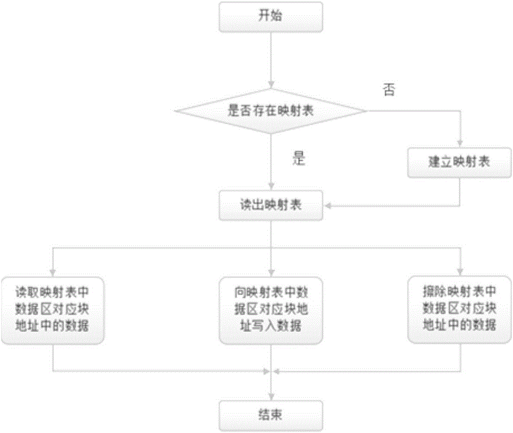
[0032] Such as figure 1 Shown, NandFlash bad block management method of the present invention comprises the following steps:

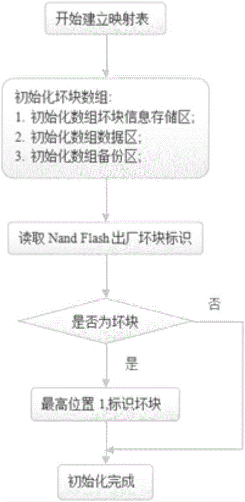
[0033] Step (1): divide the NandFlash storage device into a bad block information storage area, a data area and a backup area, and establish a bad block mapping list for recording the address mapping relationship between the bad block and its replacement block in the bad block information storage area , the replacement block of the bad block is stored in the backup area;

[0034] Step (2): detect whether the factory block flag of the NandFlash storage device is set, if so, then judge as a bad block, and store the address information of the bad block in the bad block mapping list; otherwise, enter the next step;

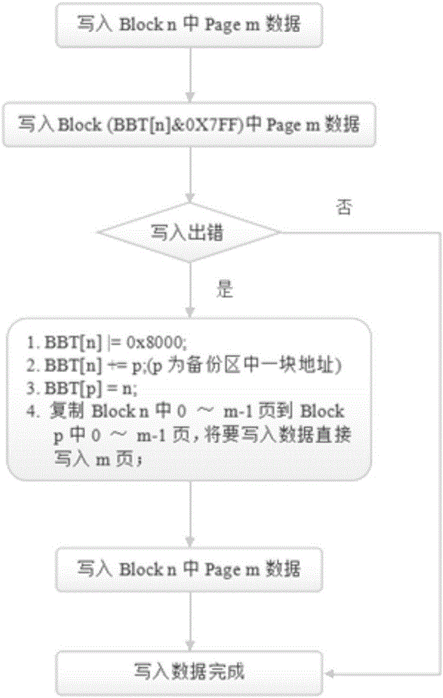
[0035] Step (3): When a bad block occurs in the current erasing / writing operation in the data area, the flag position of ...


PUM


Abstract

The invention discloses a Nand Flash bad block management method, which comprises the following steps: step (1): divide the Nand Flash storage device into a bad block information storage area, a data area and a backup area, and establish a user in the bad block information storage area. To record the bad block mapping list of the address mapping relationship between the bad block and its replacement block, the replacement block of the bad block is stored in the backup area; step (2): check whether the factory block flag of the Nand Flash storage device is set, if , it is determined to be a bad block, and the address information of the bad block is stored in the bad block mapping list; otherwise, go to the next step; Step (3): When a bad block appears in the current read / write operation in the data area, set the The flag position of the bad block is set, and the replacement block in the backup area is designated for the bad block at the same time, and the addresses of the bad block and its replacement block are stored in the bad block information table, and the bad block address in the data area is mapped to its replacement address of the block.

Description

technical field [0001] The invention belongs to the field of flash memories, in particular to a NandFlash bad block management method. Background technique [0002] NandFlash memory is a kind of flash memory, which uses a non-linear macro-cell mode inside, which provides a cheap and effective solution for the realization of solid-state large-capacity memory. Nand-flash memory has the advantages of large capacity and fast rewriting speed, and is suitable for the storage of large amounts of data, so it has been more and more widely used in the industry. For example, embedded products include digital cameras, MP3 walkman memory cards, volume Small U disk, etc. [0003] Generally, there are two methods for NandFlash to mark bad blocks: (1) Skip bad block method: The method of skipping bad blocks is to create a bad block table through an algorithm and when the target address is consistent with the bad block address, the data will be stored In the next good block, skip the bad b...

Claims


Application Information

Patent Timeline
Patent Type & Authority Applications(China)
IPC IPC(8): G06F12/06G06F12/12
CPCG06F12/0646G06F12/121
Inventor 姚舜孟祥军高彦斌李伟硕
Owner SHANDONG LUNENG SOFTWARE TECH
Why Eureka
Try Eureka