Method and apparatus for processing an optoelectronic component

A technology of optoelectronic components and equipment, applied in the field of equipment carrier, processing optoelectronic components, and computer programs, can solve problems such as high cost and unqualified optical system, and achieve the effect of avoiding readjustment

Inactive Publication Date: 2016-07-06
OSRAM OPTO SEMICON GMBH & CO OHG
View PDF4 Cites 2 Cited by
  • Summary
  • Abstract
  • Description
  • Claims
  • Application Information

AI Technical Summary

Problems solved by technology

[0004] Such optical systems are generally rejects or have to be readjusted in an expensive manner

Method used


Image

  • Method and apparatus for processing an optoelectronic component
  • Method and apparatus for processing an optoelectronic component
  • Method and apparatus for processing an optoelectronic component

Examples


Embodiment Construction

[0088] In the following, the same reference numerals may be used for the same features. Still further, for the sake of clarity, it may be provided that not all reference numerals for all elements are included in all figures.

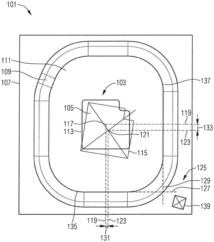
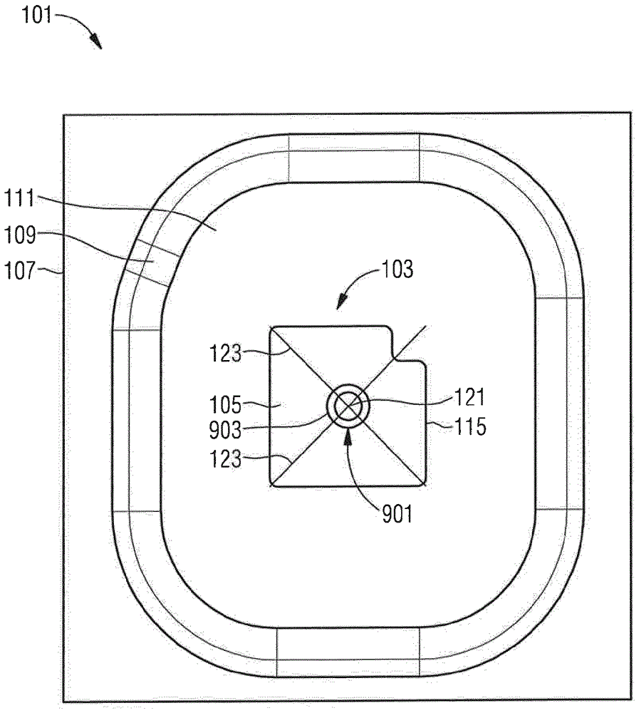
[0089] figure 1 An optoelectronic component 101 is shown.

[0090] The optoelectronic component 101 includes a light source 103 . The light source 103 has a light emitting region 105 . The light emitting area 105 is formed by means of light emitting diodes. For clarity, the light emitting diodes are not shown.

[0091] In an embodiment not shown, it may be provided that a plurality of light emitting areas are provided. In a further embodiment not shown, it may be provided that a plurality of light emitting diodes are provided for forming the light emitting area.

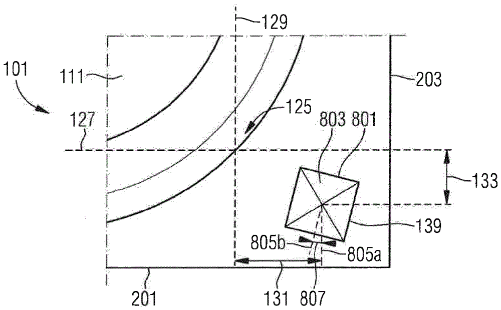
[0092]Furthermore, the optoelectronic component 101 includes a receptacle device 107 for receiving the light source 103 . The receptacle device 107 has a housing 109 in which the light ...


PUM


Abstract

The invention relates to a method for processing an optoelectronic component (101) comprising a light source (103), which has at least one luminous area (105) formed by one or a plurality of light emitting diodes, and a receptacle device (107) that receives the light source (103), comprising the following steps: determining (1101) a deviation of an actual position (115) of the light source (103) at the receptacle device (107) from a desired position (113) of the light source (103) at the receptacle device (107), forming (1103) at least one marking (139) at the receptacle device (107) which indicates the deviation. The invention furthermore relates to an apparatus (1201) for processing an optoelectronic component, to an optoelectronic component (101), to a method for equipping a carrier with an optoelectronic component, to an apparatus (1401) for equipping a carrier with an optoelectronic component, and to a computer program.

Description

technical field [0001] The present invention relates to methods and devices for processing optoelectronic components. The invention further relates to an optoelectronic component. The invention further relates to a method and a device for equipping a carrier. Furthermore, the present invention relates to a computer program. [0002] This patent application claims priority from German patent application DE 102013219087.5, the disclosure content of which is hereby incorporated by reference. Background technique [0003] Optoelectronic components generally include a plurality of light emitting diodes arranged in a housing. When optoelectronic components are incorporated into optical systems, such as fog lights or dipped beams, it is important for the light-emitting diodes to be arranged in precisely known desired positions within the housing. In the merged state, deviations from said desired position may generally have the result that the optical properties of the optical s...

Claims


Application Information

Patent Timeline
IPC IPC(8): H01L33/48H01L25/075F21S8/12F21V19/00
CPCH01L25/0753H01L2924/0002H01L33/0095H01L33/486H01L2933/0033H01L2924/00G01B11/272H01L21/67259H01L22/12H01L23/544H01L33/483H01L2223/54413
Inventor N.赫夫纳U.弗赖S.格勒奇K-J.朗
Owner OSRAM OPTO SEMICON GMBH & CO OHG
Why Eureka
Try Eureka