

Flexible pressure sensor and preparation method thereof
A pressure sensor and flexible technology, applied in the field of sensors, can solve the problems of poor stability and limited sensitivity improvement, and achieve the effects of preventing deformation, improving sensitivity, and overcoming high cost
- Summary
- Abstract
- Description
- Claims
- Application Information
AI Technical Summary
Problems solved by technology
Method used
Image

Examples
preparation example Construction
[0028] A preparation method for a flexible pressure sensor, specifically comprising the following steps:
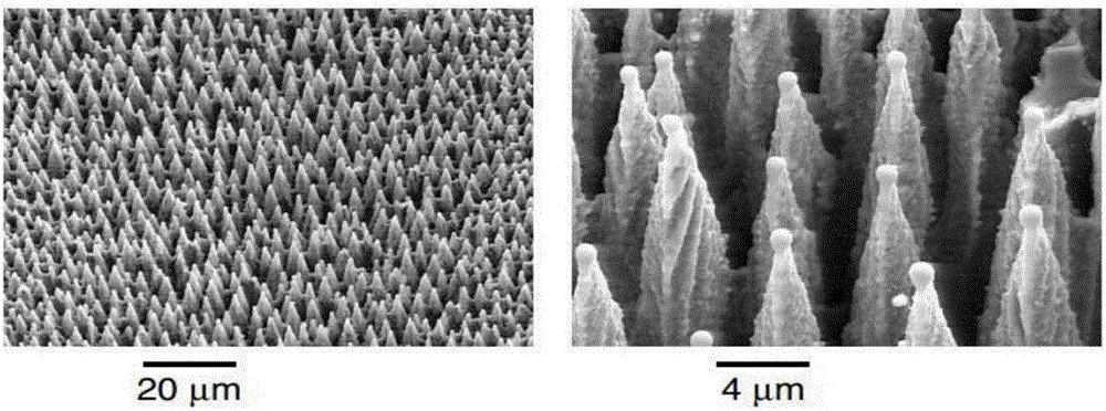
[0029] Step 1. Preparation of the first micro-nano structured PDMS film and the first CNT film: a) Cut a 6-inch silicon wafer into a size of 3cm×3cm, then ultrasonically clean it in acetone and ethanol for 15-30min, and then use deionized water Rinse and blow dry with nitrogen; b) Place the silicon wafer cleaned and dried in the previous step in the vacuum chamber of the three-dimensional mobile platform, and the vacuum chamber is filled with SF 4 After gas, when the energy density is 0.42J / cm 2 , the number of pulses is 612.5, and the energy is 0.1mJ femtosecond laser scanning and ablation at a speed of 1mm / s to obtain black silicon. The SEM image is as follows figure 2as shown; c) The black silicon obtained in the previous step was ultrasonically cleaned in acetone, absolute ethanol and deionized water for 15 to 30 minutes in sequence, and after being blown dry with ni...
Embodiment
[0034] A preparation method for a flexible pressure sensor, specifically comprising the following steps:
[0035] Step 1. Prepare the first micro-nano structured PDMS film and the first CNT film: a) Cut a 6-inch silicon wafer into a size of 3cm×3cm, then ultrasonically clean it in acetone and ethanol for 15min, and then rinse it with deionized water. Blow dry with nitrogen; b) Place the silicon wafer cleaned and dried in the previous step in the vacuum chamber of the three-dimensional mobile platform, and the vacuum chamber is filled with SF 4 After gas, when the energy density is 0.42J / cm 2 , the number of pulses is 612.5, and the energy is 0.1mJ femtosecond laser scanning and ablation at a speed of 1mm / s to obtain black silicon. The SEM image is as follows figure 2 As shown; c) The black silicon obtained in the previous step was ultrasonically cleaned in acetone, absolute ethanol and deionized water for 15 minutes in sequence, dried with nitrogen, soaked in TMCS (trimethylc...
PUM
| Property | Measurement | Unit |
|---|---|---|
| Thickness | aaaaa | aaaaa |
| Thickness | aaaaa | aaaaa |
| Thickness | aaaaa | aaaaa |
Abstract
Description
Claims
Application Information