A High-Speed Review Method for Microscopic Defects
A high-speed, defect-free technology, applied in the field of optical inspection, can solve problems such as unstable focus and sensor vibration, and achieve the effect of shortening time and high efficiency of re-examination and taking pictures
- Summary
- Abstract
- Description
- Claims
- Application Information
AI Technical Summary
Problems solved by technology
Method used
Image
Examples
Embodiment Construction
[0017] The specific implementation manner of the present invention will be described in further detail below by describing the embodiments with reference to the accompanying drawings.
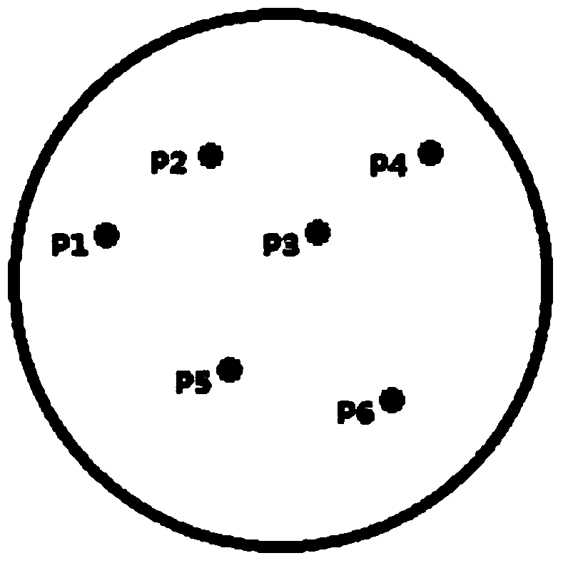
[0018] Use a line scan camera (or an area scan camera with a strobe) to perform low-magnification (1x-5x) image scanning to find the position of the defect on the surface of the inspected object (such as: wafer, flat glass or biomedical slice).
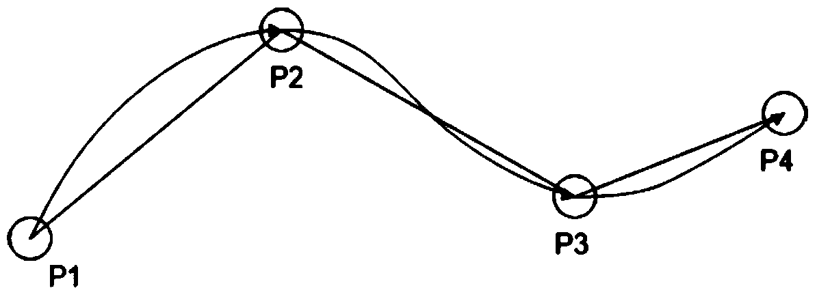
[0019] Such as figure 2 As shown, the defect points on the product are connected into a curve; for example, the four defect points P1, P2, P3, and P4 are connected into a curve in turn, and the camera passes through the four defect points of P1, P2, P3, and P4 along the curve in turn. Take high-speed photography.
[0020] A high-speed area scan camera (CCD or CMOS sensor) equipped with a high-magnification (20x-50x) microscope lens moves at a constant speed along the curve formed by the defect points, and the camera's auto-focus is always on; when ea...
PUM
 Abstract
Description
Claims
Application Information

