
Manufacturing method of no-easy-warpage large-dimension light emitting diode epitaxial wafer

A technology of light-emitting diodes and manufacturing methods, which is applied to electrical components, circuits, semiconductor devices, etc., and can solve problems such as increased warpage, abnormal epitaxial surface, and abnormal electrical properties

Active Publication Date: 2016-07-20
XIAMEN CHANGELIGHT CO LTD
View PDF3 Cites 3 Cited by
  • Summary
  • Abstract
  • Description
  • Claims
  • Application Information

AI Technical Summary

Problems solved by technology

[0005] The purpose of the present invention is to provide a large-size light-emitting diode epitaxial wafer manufacturing method that is not prone to warping, so as to solve the problem of epitaxial surface anomalies and electrical properties caused by temperature changes in the process of growing epitaxial wafers due to temperature changes. abnormal problem

Method used


Image

  • Manufacturing method of no-easy-warpage large-dimension light emitting diode epitaxial wafer
  • Manufacturing method of no-easy-warpage large-dimension light emitting diode epitaxial wafer
  • Manufacturing method of no-easy-warpage large-dimension light emitting diode epitaxial wafer

Examples


Embodiment Construction

[0049] The present invention will be described in detail below in conjunction with the accompanying drawings and specific embodiments.

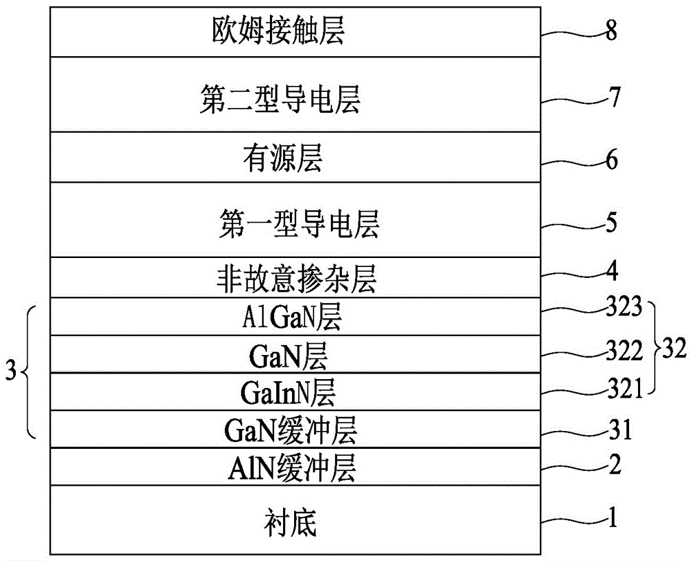
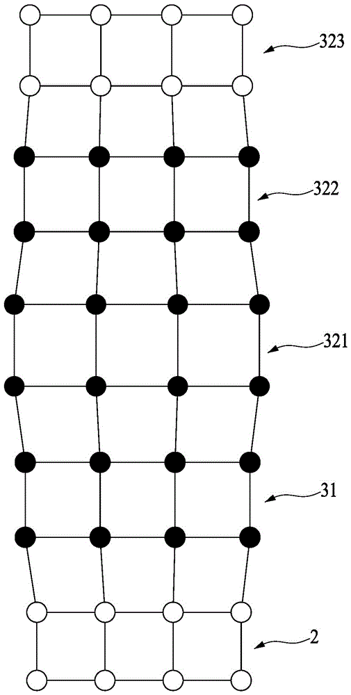
[0050] refer to image 3 and Figure 4As shown, the present invention discloses a large-scale light-emitting diode epitaxial wafer that is not easy to warp. AlN buffer layer 2 is grown on substrate 1, composite buffer layer 3 is grown on AlN buffer layer 2, and unintentional buffer layer 3 is grown on composite buffer layer 3. A doped layer (uGaN) 4, a first-type conductive layer (nGaN) 5 grown on the unintentionally doped layer 4, an active layer 6 grown on the first-type conductive layer 5, and a second-type conductive layer grown on the active layer 6 7. An ohmic contact layer 8 is grown on the second-type conductive layer 7 . The substrate 1 is preferably a large-scale sapphire substrate. An electron blocking layer may be grown between the active layer 6 and the second-type conductive layer 7 .

[0051] The composite buffer layer 3 is...


PUM

PropertyMeasurementUnit
thicknessaaaaaaaaaa
thicknessaaaaaaaaaa
thicknessaaaaaaaaaa

Abstract

The invention discloses a manufacturing method of a no-easy-warpage large-dimension light emitting diode epitaxial wafer. The manufacturing method comprises the steps of performing vapor plating of an AlN buffer layer on the upper surface of a substrate; performing epitaxial growth of a GaN buffer layer on the AlN buffer layer; performing epitaxial growth of a composite buffer layer on the GaN buffer layer at a reaction temperature of about 1000 DEG C, wherein the composite buffer layer is composed of a GaN buffer layer and multiple buffer layers; after growth of the composite buffer layer, increasing the epitaxial growth temperature to above 1050 DEG C for realizing successive epitaxial growth of an unintentional doping layer and a first type conductive layer; reducing the epitaxial growth temperature to lower than 800 DEG C and performing epitaxial growth of an active layer on the first type conductive layer; and increasing the temperature to above 900 DEG C and successively growing a second type conductive layer and an ohmic contact layer on the active layer. The manufacturing method settles problems of epitaxial surface abnormity and electrical performance abnormity because of large warpage caused by temperature change in epitaxial wafer growth process in which the large-dimension substrate is utilized.

Description

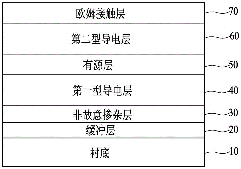
technical field [0001] The invention relates to the technical field of light-emitting diodes, in particular to a method for manufacturing a large-size light-emitting diode epitaxial wafer that is not prone to warping. Background technique [0002] Such as figure 1 As shown, in the structure of the traditional large-scale light-emitting diode epitaxial wafer disclosed in the prior art, a buffer layer 20 is evaporated by PVD on the large-scale substrate 10, and the buffer layer 20 is an AlN buffer layer, or a GaN buffer layer, or An AlGaN buffer layer; growing an unintentionally doped layer (uGaN) 30 on the buffer layer 20; growing a first-type conductive layer (nGaN) 40 on the unintentionally doped layer 30; growing a first-type conductive layer (nGaN) 40 An active layer (MQW) 50 is grown on it; a second-type conductive layer (pGaN) 60 is grown on the active layer (MQW) 50 ; an ohmic contact layer (ITO) 70 is grown on the second-type conductive layer (pGaN) 60 . [0003] Su...

Claims


Application Information

Patent Timeline
Patent Type & Authority Applications(China)
IPC IPC(8): H01L33/12H01L33/00
CPCH01L33/005H01L33/12
Inventor 林志伟陈凯轩张永汪洋卓祥景姜伟童吉楚方天足
Owner XIAMEN CHANGELIGHT CO LTD
Learn More