Back alignment measurement system
A measurement system and silicon wafer alignment technology, applied in the field of integrated circuit equipment manufacturing, can solve the problems of small number of marks and strong position constraints, and achieve the effect of improving alignment accuracy and avoiding poor adaptability
- Summary
- Abstract
- Description
- Claims
- Application Information
AI Technical Summary
Problems solved by technology
Method used
Image

Examples
Embodiment Construction
[0029] Specific embodiments of the present invention will be described in detail below in conjunction with the accompanying drawings.
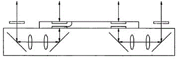
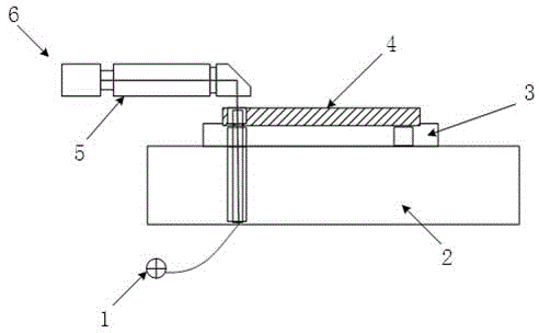
[0030] figure 2 It is a schematic diagram of the structure of the back alignment device of the present invention. Such as figure 2 As shown, the device is composed of six parts including a workpiece table 2, a silicon wafer adsorption table 3, a rear alignment imaging lens 5, a CCD camera 6, a transmission infrared light source 1 and a controller. The workpiece table 2 fixes the silicon wafer adsorption table chuck3, and moves the window to the field of view of the imaging lens 5. The silicon wafer adsorption table chuck3 absorbs the silicon wafer 4 and drives the silicon wafer 4 to rotate. The light source 1 is a transmissive infrared light source for penetrating the silicon chip and forming an image on the lens object side. The image of the object plane is imaged on the CCD6 target surface by the infrared alignment imaging lens 5 . Th...
PUM
 Abstract
Description
Claims
Application Information
 - R&D
- Intellectual Property
- Life Sciences
- Materials
- Tech Scout
- Unparalleled Data Quality
- Higher Quality Content
- 60% Fewer Hallucinations
Browse by: Latest US Patents, China's latest patents, Technical Efficacy Thesaurus, Application Domain, Technology Topic, Popular Technical Reports.
© 2025 PatSnap. All rights reserved.Legal|Privacy policy|Modern Slavery Act Transparency Statement|Sitemap|About US| Contact US: help@patsnap.com