Automatic focusing system for scanning electron microscope equipped with laser defect detection function

a scanning electron microscope and automatic focusing technology, which is applied in the direction of semiconductor/solid-state device testing/measurement, instruments, and super-high-integrated lsis manufacturing, can solve the problems of micro foreign matter with diameters of 0.1 .lambda.m, defects in semiconductor chips and their lowering quality and reliability, and defective products in manufacturing super-highly integrated lsis

Inactive Publication Date: 2003-09-16
HITACHI HIGH TECH SCI CORP
View PDF6 Cites 114 Cited by
  • Summary
  • Abstract
  • Description
  • Claims
  • Application Information

AI Technical Summary

Problems solved by technology

A major factor that leads to defective products in manufacturing super-highly integrated LSIs in recent years is said to result from by micro foreign matters that adhere to wafers.
More particularly, the micro foreign matters turn into pollutants that cause breakage and short circuit of circuit patterns, which lead to a great extent to occurrence of defects in semiconductor chips and their lowered quality and reliability.
With the miniaturization of circuit patterns, micro foreign matters having diameters on the order of 0.1 .lambda.m could be problematical.
However, in the defect detection method in which an optical microscope is used to observe scattered light of a laser beam, since the focal depth of the optical system is deep, defects can be detected to some degree even when the focal point of the optical microscope is not located on the wafer surface.
However, since the scanning electron microscope has a shallow focal depth, it is difficult to observe defects in the size of 0.1 .mu.m when the focusing surface shifts by 10 .mu.m or more.
For this reason, when defects are spotted with the laser beam, and such defects are to be observed by a scanning electron microscope, the defects may often move out of the focal point of the scanning electron microscope.
Moreover, since defects to be observed are extremely small, it would take a substantially long time to readjust the focus, which deteriorates the work efficiency.

Method used


Image

  • Automatic focusing system for scanning electron microscope equipped with laser defect detection function
  • Automatic focusing system for scanning electron microscope equipped with laser defect detection function
  • Automatic focusing system for scanning electron microscope equipped with laser defect detection function

Examples


Embodiment Construction

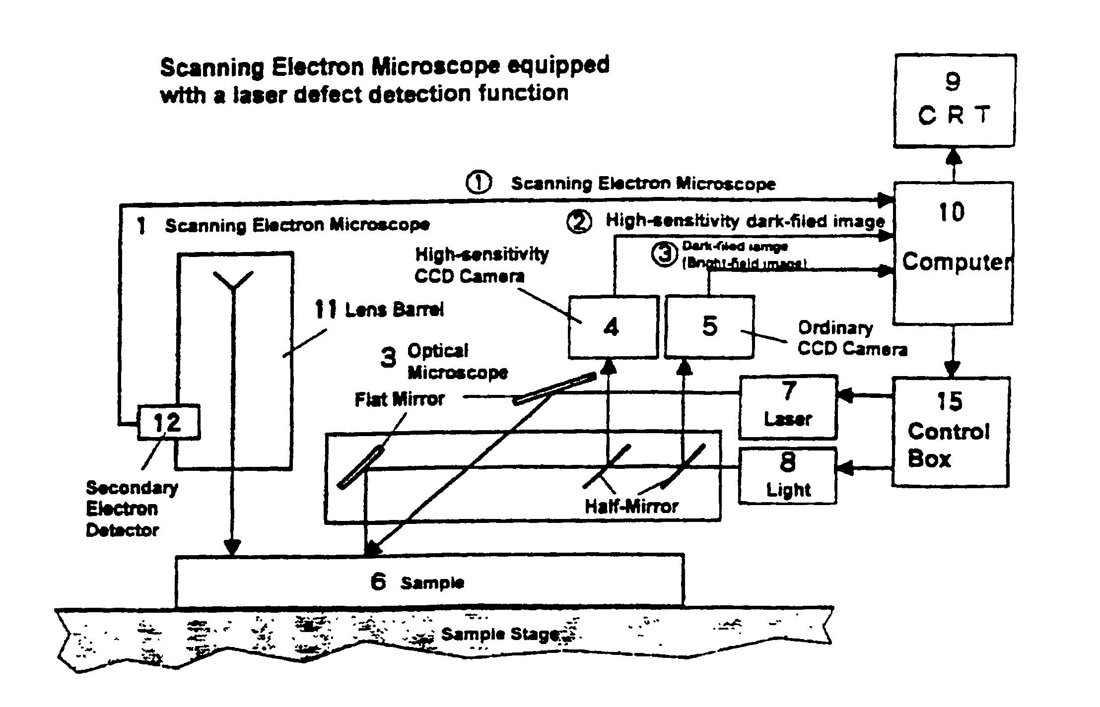
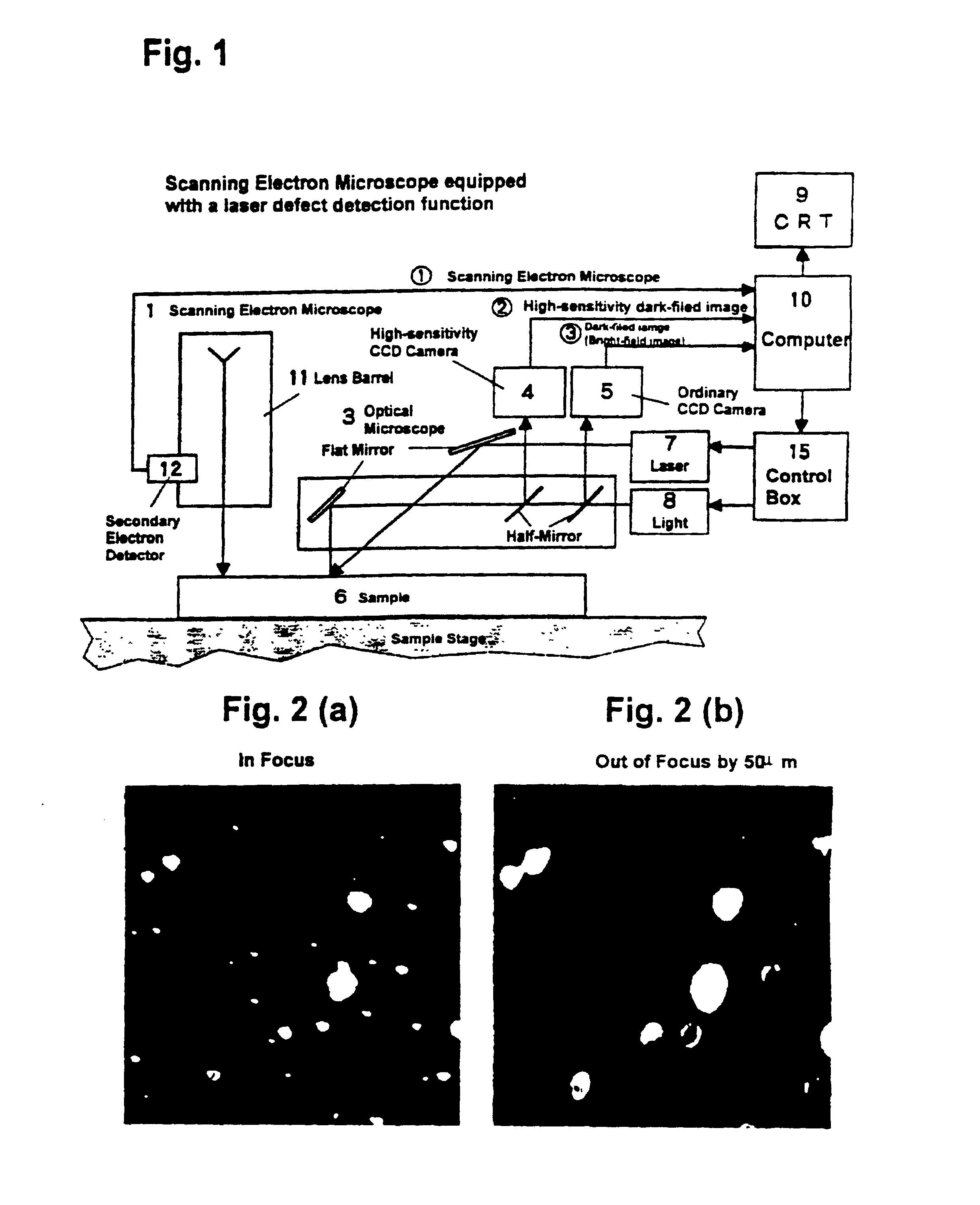
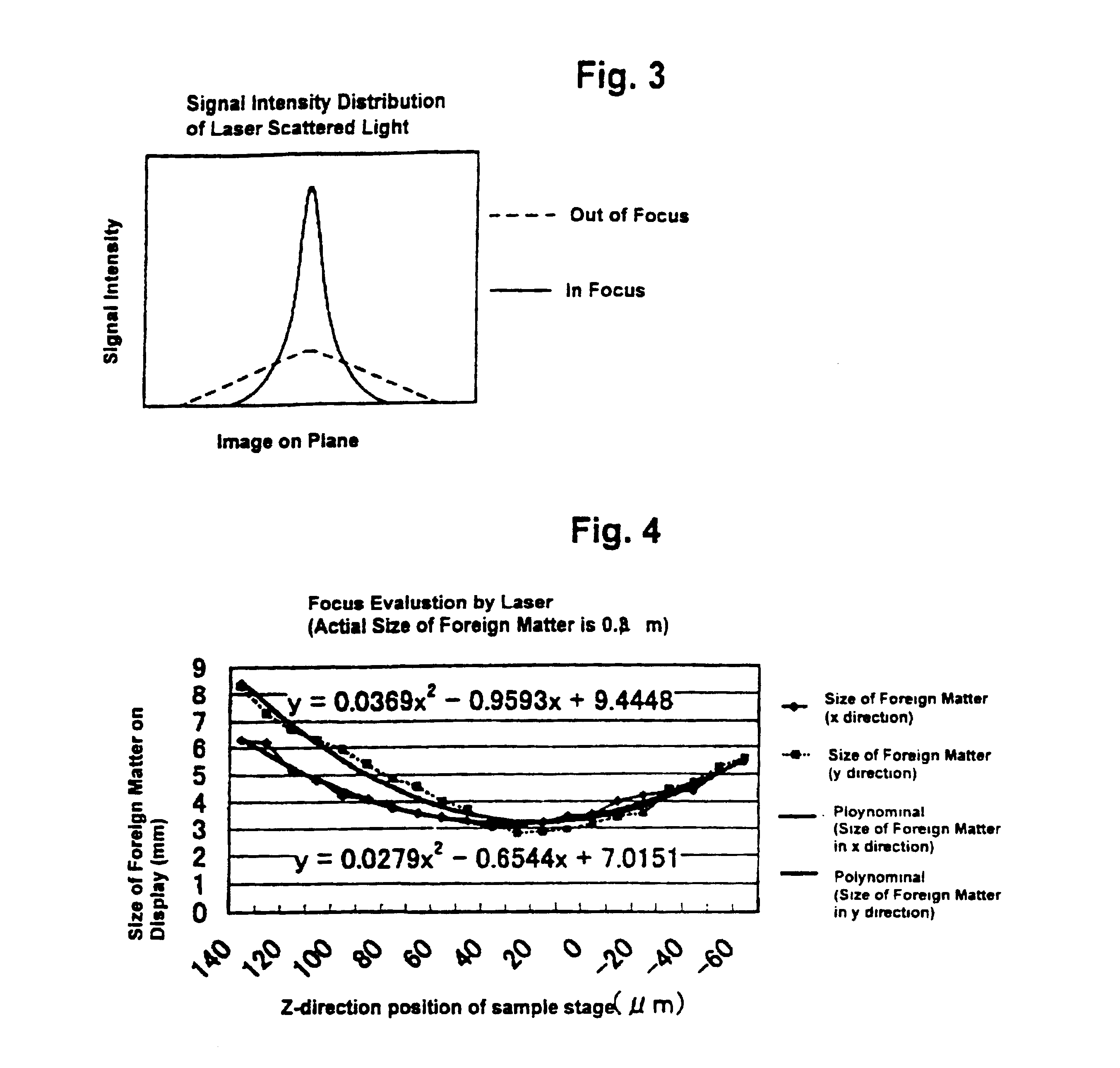
Minute foreign matters that are present on a surface of a planate sample such as a silicon wafer can be detected by using a scanning electron microscope equipped with a laser defect detection function and analyzed. However, when minute foreign matters whose positions have been specified by a dark-field image obtained by the laser irradiation are subject to an observation by the scanning electron microscope, such observation may not be immediately conducted as it may take time to readjust the image. As described above, in the case of a scanning electron microscope, an image formed by the scanning electron microscope is blurred when the image is not in focus because its focal depth is shallow. Observation of extremely small particles is thus impossible if the image is not in focus.

In accordance with an embodiment of the present invention, a scanning electron microscope is provided with an automatic focusing function so that observation by the scanning electron microscope can be quickl...


PUM

PropertyMeasurementUnit
sizeaaaaaaaaaa
sizeaaaaaaaaaa
sizeaaaaaaaaaa

Abstract

A scanning electron microscope equipped with a laser defect detection function has an automatic focusing function that performs the steps of: obtaining a deviation (offset) amount between focal positions of an optical microscope and a scanning electron microscope; detecting a defect by a laser dark-field image of the optical microscope; analyzing the dark-field image to readjust a focus of the optical microscope to adjust a height of the optical microscope; and automatically adjusting a focus of the scanning electron microscope by adding a readjusted amount of the focus of the optical microscope to the offset amount before an observation is conducted by the scanning electron microscope.

Description

1. Field of the InventionThe present invention relates to an automatic focusing system for a scanning electron microscope equipped with a laser defect detection function, which is used to control the yield in semiconductor manufacturing processes.2. Related Background ArtA major factor that leads to defective products in manufacturing super-highly integrated LSIs in recent years is said to result from by micro foreign matters that adhere to wafers. More particularly, the micro foreign matters turn into pollutants that cause breakage and short circuit of circuit patterns, which lead to a great extent to occurrence of defects in semiconductor chips and their lowered quality and reliability. With the miniaturization of circuit patterns, micro foreign matters having diameters on the order of 0.1 .lambda.m could be problematical. For this reason, it has become the most important objective, for controlling the process and improving yield in manufacturing super-highly integrated LSIs, to q...

Claims


Application Information

Patent Timeline
Patent Type & Authority Patents(United States)
IPC IPC(8): H01J37/02H01J37/21H01J37/22G01Q20/00G01Q30/02G01Q30/06G01R31/02G01R31/302G02B21/00H01L21/66
CPCH01J37/21H01J37/226H01J2237/216
Inventor MORITA, SEIJISATO, MITSUYOSHIUEMOTO, ATSUSHI
Owner HITACHI HIGH TECH SCI CORP
Why Eureka
Try Eureka