JFET and manufacturing method thereof

A manufacturing method and technology of conductivity type, applied in semiconductor/solid-state device manufacturing, electrical components, electrical solid-state devices, etc., can solve the problems of unstable performance of JFET, large changes in substrate resistivity, low doping concentration, etc.

Active Publication Date: 2016-07-27
SHANGHAI HUAHONG GRACE SEMICON MFG CORP
View PDF4 Cites 8 Cited by
  • Summary
  • Abstract
  • Description
  • Claims
  • Application Information

AI Technical Summary

Problems solved by technology

[0005] Ultra-high voltage JFETs all use ultra-high resistance substrates, and the doping concentration is ve

Method used


Image

  • JFET and manufacturing method thereof
  • JFET and manufacturing method thereof
  • JFET and manufacturing method thereof

Examples


Embodiment Construction

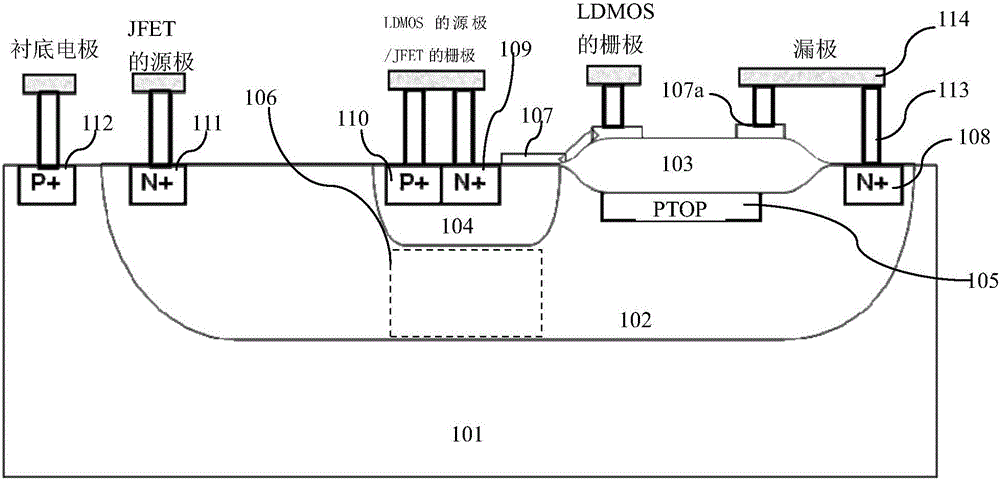
[0065] like figure 1 Shown is a schematic structural diagram of an existing JFET; JFET is integrated in LDMOS, taking an N-type device as an example, an N-type deep well 102 is formed in a P-type semiconductor substrate such as a P-type silicon substrate 101, and an N-type deep well 102 is formed in a P-type semiconductor substrate such as a P-type silicon substrate 101. A field oxide layer 103 is formed on the surface of the P-type silicon substrate 101 of the P-type deep well 102 . The P-type well region 104 is formed in the N-type deep well 102, and the P-type well region 104 is simultaneously used as the channel region of the LDMOS and the gate region of the JFET; a PTOP is formed on the surface of the N-type deep well 102 at the bottom of the field oxide layer 103 Layer 105. The N+ doped drain region 108 shared by JFET and LDMOS is formed on the surface of N-type deep well 102, and the drift region shared by JFET and LDMOS is composed of N-type deep well 102 between drai...


PUM


Abstract

The invention discloses a JFET integrated in an LDMOS. A grid electrode region of the JFET is simultaneously used as a channel region of the LDMOS. The JFET and the LDMOS share a drift region and a drain region. A deep trap at the bottom part of the grid electrode region of the JFET forms a channel region of the JFET. A source region and the drain region of the JFET are respectively arranged at two sides of the channel region of the JFET. A source region of the JFET is formed on the surface of the deep trap. A second conductive type buried layer is formed at the position of a first conductively type deep trap at the bottom part of the channel region of the JFET and at the junction position of a second conductive type semiconductor substrate. The buried layer and the grid electrode region of the JFET realize the consumption of the channel region of the JFET together, and the fluctuation of the channel region consumption of the JFET, which is caused by the fluctuation of the doped concentration of the substrate when the substrate and the bottom part of the channel region of the JFET directly contact, is eliminated, so that the stability of the device is improved. The invention further discloses a manufacturing method of the JFET.

Description

technical field [0001] The invention relates to the field of semiconductor integrated circuit manufacturing, in particular to a junction field effect transistor (JFET). The invention also relates to a method for manufacturing a JFET. Background technique [0002] JFET uses the PN junction as the gate of the device to control the opening and closing of the channel. When the PN junction is negatively biased on the gate, both sides of the PN junction are depleted. When the channel is completely depleted, the device is in the pinch-off state of the channel. due. Otherwise, the device turns on. [0003] The ultra-high voltage junction field effect transistor needs the drain to withstand high voltage. Usually, the drift region of high-voltage LDMOS is used as the drift region of JFET to withstand high voltage, and the channel of high-voltage LDMOS is used as the gate of JFET. In this way, ultra-high voltage JFET can be produced, and the Share the photolithography plate with hig...

Claims


Application Information

Patent Timeline
IPC IPC(8): H01L27/07H01L29/10H01L29/78H01L29/808H01L21/8232
CPCH01L21/8232H01L27/0705H01L29/1058H01L29/7817H01L29/808
Inventor 钱文生
Owner SHANGHAI HUAHONG GRACE SEMICON MFG CORP
Why Eureka
Try Eureka