Novel P<+> sidewall non-junction field effect transistor

A junction field effect and transistor technology, which is applied in the field of new P+ sidewall junctionless field effect transistors, can solve the problems of limited leakage current control of junctionless devices, insufficient leakage current control ability, and inability to form greater control capabilities.

Active Publication Date: 2016-07-27
HANGZHOU DIANZI UNIV
View PDF4 Cites 2 Cited by
  • Summary
  • Abstract
  • Description
  • Claims
  • Application Information

AI Technical Summary

Problems solved by technology

However, despite the use of high-K materials, the gate's ability to control this part of the extra channel is very limited. When the device gate continues to shrink, the leakage current control is still not enough
[0005] Based on the understanding and ma

Method used


Image

  • Novel P&lt;+&gt; sidewall non-junction field effect transistor
  • Novel P&lt;+&gt; sidewall non-junction field effect transistor
  • Novel P&lt;+&gt; sidewall non-junction field effect transistor

Examples


Embodiment Construction

[0015] In order to make the purpose, technical solution and advantages of the present invention clearer, the present invention will be described in detail below in conjunction with the accompanying drawings.

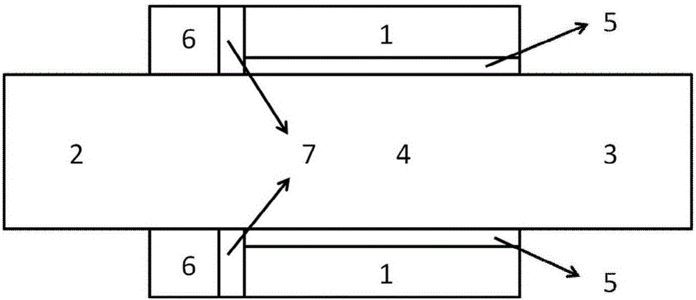
[0016] Such as figure 1 As shown, a new type of P + Sidewall junctionless field effect transistor, including double gate 1, source region 2, drain region 3, channel region 4, gate dielectric layer 5, P + Sidewall 6 and isolation layer 7; wherein, the double gate 1 is located at the upper and lower positions of the channel region 4, and maintains vertical symmetry, the gate dielectric layer 5 is located between the channel region 4 of the double gate 1, and the double gate 1 One side with P + Side wall 6, P + The side wall 6 is a symmetrical structure up and down, and the double gate 1 and the P + An isolation layer 7 is provided between the side walls 6, P + The sidewall 6 is in direct contact with the source region 2 . The doping concentration of source region 2, ...


PUM


Abstract

The invention discloses a P<+> sidewall non-junction device. The P<+> sidewall non-junction device consists of dual gates, a source region, a drain region, a channel region, gate dielectric layers, P<+> sidewalls and isolation layers. For a conventional non-junction device, when the length of a gate is reduced to 10nm, a leakage current is greatly increased, so that the inhibition of the magnitude of the leakage current becomes an important task of a small-sized device. For the conventional non-junction device, a turn-off current of the device in a turn-off state cannot be effectively controlled only by the control capability of the gate. According to the P<+> sidewall non-junction device, PN junction depletion can be formed for assisting in depletion of the device, and when the device is turned on, the gate controls a P<+> region for weakening the PN junction depletion, so that a turn-on current is not influenced. Compared with the conventional non-junction device, the novel P<+> sidewall tri-gate nanowire non-junction device has great advantages, and the advantages are especially remarkable when the gate is very short. The novel device mainly can improve the characteristics of a sub-threshold slope, a turn-on and turn-off current ratio and the like of the conventional non-junction device.

Description

technical field [0001] The invention relates to a device for semiconductor integrated circuits, mainly a novel P+ side wall junctionless field effect transistor. Background technique [0002] As the size of the device decreases, the leakage current of the device will gradually increase, which causes a great degradation of the characteristics of the device. Therefore, finding ways to reduce the leakage current of small junction-free devices has become a top priority. There are few methods that can reduce the leakage current of the device, and the more common one is to increase the control ability of the gate. In addition to the modification of the device gate, we hope that the leakage current of the junction-free device can be reduced through the modification of the side wall of the device. Sidewalls usually use SiO 2 and other materials to isolate the gate and source and drain regions. We hope that the sidewall can play a greater role in device cut-off. By modifying the...

Claims


Application Information

Patent Timeline
IPC IPC(8): H01L29/78H01L29/423
CPCH01L29/42356H01L29/7831
Inventor 王颖孙玲玲唐琰曹菲
Owner HANGZHOU DIANZI UNIV
Why Eureka
Try Eureka