Thin film transistor, display substrate and liquid crystal display device

A technology of thin film transistor and substrate substrate, applied in the field of liquid crystal display, can solve the problems of low on-current I-on, unfavorable development of liquid crystal display panel, large off-current I-off, etc., so as to avoid thin film transistors, electrons and holes. The effect of uniform distribution and low shutdown current

Inactive Publication Date: 2016-10-12
BOE TECH GRP CO LTD +1
View PDF5 Cites 11 Cited by
  • Summary
  • Abstract
  • Description
  • Claims
  • Application Information

AI Technical Summary

Problems solved by technology

[0004] However, the thin film transistors of the prior art have relatively low turn-on current I-on and relatively large turn-of

Method used


Image

  • Thin film transistor, display substrate and liquid crystal display device
  • Thin film transistor, display substrate and liquid crystal display device
  • Thin film transistor, display substrate and liquid crystal display device

Examples


Embodiment Construction

[0026] The implementation process of the embodiment of the present application will be described in detail below in conjunction with the accompanying drawings. It should be noted that the same or similar reference numerals represent the same or similar elements or elements having the same or similar functions throughout. The embodiments described below by referring to the figures are exemplary, and are only for explaining the present application, and should not be construed as limiting the present application.

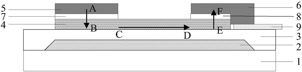
[0027] figure 1 Shown is a schematic structural diagram of a bottom-gate thin-film transistor of the prior art TFT-LCD, wherein the thin-film transistor is provided with a gate 2 on a base substrate 1, a gate insulating layer 3 is provided on the gate 2, and An active layer 4 is arranged on the gate insulating layer 3, a source electrode 5 and a drain electrode 6 are arranged on the active layer 4, and an improved gap between the source electrode 5 and the active laye...


PUM


Abstract

The present application provides a thin film transistor, a display substrate and a liquid crystal display device, so as to increase the turn-on current of the thin film transistor and reduce the turn-off current of the thin film transistor. The thin film transistor provided by the present application includes: a gate electrode, a gate insulating layer, and an active layer arranged on the substrate in sequence, and also includes: a source electrode arranged on the active layer, and an electrode arranged on the The drain between the gate insulating layer and the active layer.

Description

technical field [0001] The present application relates to the field of liquid crystal display, in particular to a thin film transistor, a display substrate and a liquid crystal display device. Background technique [0002] Thin Film Transistor Liquid Crystal Display (TFT-LCD) has the characteristics of small size, low power consumption, no radiation, and relatively low manufacturing cost, and occupies a dominant position in the current flat panel display market. [0003] The bottom-gate thin film transistor of the prior art TFT-LCD usually includes a gate, a gate insulating layer, an active layer, a source and a drain which are sequentially located on the substrate, wherein the source and the drain are usually arranged on the same layer. When the gate is connected to a high level, the electrons in the active layer usually move downward, forming an electronic conductive layer on the surface close to the gate, and the electrons in the source pass through the conductive layer ...

Claims


Application Information

Patent Timeline
IPC IPC(8): H01L29/786H01L27/12H01L21/336
CPCH01L29/78618H01L27/12H01L29/66227
Inventor 裴晓光赵海生肖红玺蒋会刚肖志莲刘冲林子锦
Owner BOE TECH GRP CO LTD
Why Eureka
Try Eureka