Quasicrystal patterning transparent film electrode used for intelligent light modulation film

A transparent conductive film, intelligent dimming technology, used in circuits, electrical components, semiconductor devices, etc.

Active Publication Date: 2016-07-27
北京京城鸿业科技有限公司
View PDF8 Cites 8 Cited by
  • Summary
  • Abstract
  • Description
  • Claims
  • Application Information

AI Technical Summary

Problems solved by technology

[0007] In order to solve the above technical problems, especially the low conductivity of traditional graphene, the optical interference caused by the metal grid structure in traditional composite films, etc.

Method used


Image

  • Quasicrystal patterning transparent film electrode used for intelligent light modulation film
  • Quasicrystal patterning transparent film electrode used for intelligent light modulation film
  • Quasicrystal patterning transparent film electrode used for intelligent light modulation film

Examples


Embodiment 1

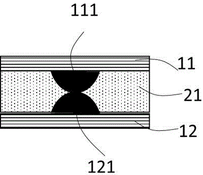
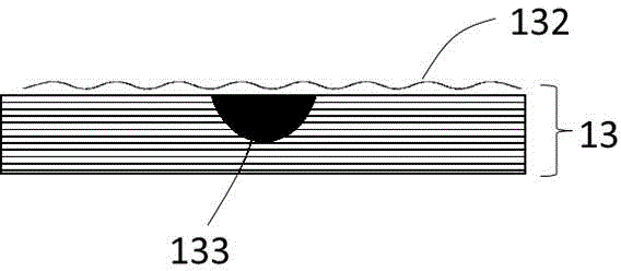
[0049] Preparation of graphene / embedded quasicrystal patterned silver metal mesh composite transparent conductive thin film electrode

[0050] 1. Fabrication of Embedded Quasicrystalline Patterned Silver Metal Grids

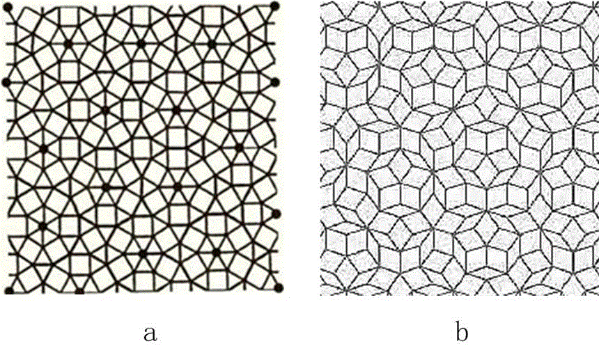
[0051] Coat a layer of UV-cured polymethyl methacrylate (PMMA Xinguang SKA-HC-1) on a 5cm*5cm PET (AICA, model HC2106) substrate, and then use the grid template (self-made, height is 10μm, the side length is 1mm, and the line width is 50μm, the shape is selected from figure 1 (b) The pattern shown) was placed on the PMMA glue and then cured by UV. After curing, the template is peeled off, and the conductive silver paste (Suzhou Lengshi, SNP-MM-03) is further filled in the groove part with a scraper, and the excess silver paste is scraped off with a scraper after filling. Then put the prepared plate into an oven at 150° C. and bake for 30 minutes. Its preparation process is as follows Figure 7 shown.

[0052] 2. Preparation of Graphene Layer

[0053] Put...

Embodiment 2

[0056] With the grid template of step 1 in Example 1, the parameters are set as a grid with a height of 10 μm, a side length of 0.5 mm, and a line width of 50 μm, and the remaining steps are consistent with Example 1 to prepare graphene / embedded quasicrystals Patterned silver metal mesh composite graphene transparent conductive film electrodes.

Embodiment 3

[0058] With the grid template of step 1 in Example 1, the parameters are set to a grid with a height of 10 μm, a side length of 2 mm, and a line width of 50 μm, and the remaining steps are consistent with Example 1 to prepare graphene / embedded quasicrystal patterns Silver metal grid composite transparent conductive film electrode.


PUM

PropertyMeasurementUnit
thicknessaaaaaaaaaa
electron mobilityaaaaaaaaaa
electrical resistivityaaaaaaaaaa

Abstract

The invention discloses a quasicrystal patterning transparent film electrode used for an intelligent light modulation film and a preparation method for the same, and a related intelligent modulation film and a preparation method for the same. The quasicrystal patterning transparent film electrode is a graphene / quasicrystal patterning metal mesh composite transparent conductive film electrode; the graphene / quasicrystal patterning metal mesh composite transparent conductive film electrode consists of a substrate, a quasicrystal patterning metal mesh and a graphene layer; the intelligent light modulation films consists of two graphene / quasicrystal patterning metal mesh composite transparent conductive film electrodes which are opposite in a staggermanner and a light ray modulation unit clamped between the two graphene / quasicrystal patterning metal mesh composite transparent conductive film electrodes, wherein the light ray modulation layer is doped with a backing, the stagger portion is provided with a lead out electrode, and the device is packaged by a packaging material. The graphene / quasicrystal patterning metal mesh composite transparent conductive film electrode can effectively eliminate the optical effect produced by the metal grid in the light modulation film and enables the light modulation film to be applied in the light modulation device having higher requirements.

Description

Technical field: [0001] The invention relates to a transparent conductive film, an intelligent dimming film and a preparation method thereof, in particular to a transparent conductive thin film electrode for an intelligent dimming film and a preparation method thereof, and a related intelligent dimming film and a preparation method thereof. Background technique: [0002] Smart dimming film is a photoelectric device that changes its optical parameters such as light transmittance and haze through the input of electrical signals. It is often used in building exterior walls, real estate decoration, automobile glass, automobile rearview mirrors, projection curtain walls, office spaces, public entertainment facilities and other fields. Taking the smart window on the building as the most typical application of smart dimming film as an example, the smart dimming film is combined with architectural glass by sticking, clamping, etc. The intensity of incident light can be reduced to...

Claims


Application Information

Patent Timeline
Patent Type & Authority Applications(China)
IPC IPC(8): H01L31/0224H01L31/18
CPCY02P70/50
Inventor 赵庆生王丽霞刘腾蛟胡源高阳
Owner 北京京城鸿业科技有限公司
Why Eureka
Try Eureka