NAND Flash fault-tolerance method based on FPGA (Field Programmable Gate Array)

A content and bad block technology, applied in the field of Flash fault tolerance, can solve problems such as data cannot be read and written normally, Flash scrapping, system instability, etc., to solve the problem of bad block detection and management, improve storage performance, The effect of ensuring data security

Active Publication Date: 2016-08-10
ZHEJIANG UNIV
View PDF4 Cites 16 Cited by
  • Summary
  • Abstract
  • Description
  • Claims
  • Application Information

AI Technical Summary

Problems solved by technology

[0003] Since the technology of NAND Flash cannot guarantee the reliable performance of NAND Memory Array during its life cycle, there will be invalid blocks that cannot be erased during use and use, that is, bad blocks
The bad blocks that existed at the time of release cannot be used to store data, and have been mark

Method used


Image

  • NAND Flash fault-tolerance method based on FPGA (Field Programmable Gate Array)
  • NAND Flash fault-tolerance method based on FPGA (Field Programmable Gate Array)
  • NAND Flash fault-tolerance method based on FPGA (Field Programmable Gate Array)

Examples


Embodiment Construction

[0031] The present invention will be further described below in conjunction with drawings and embodiments.

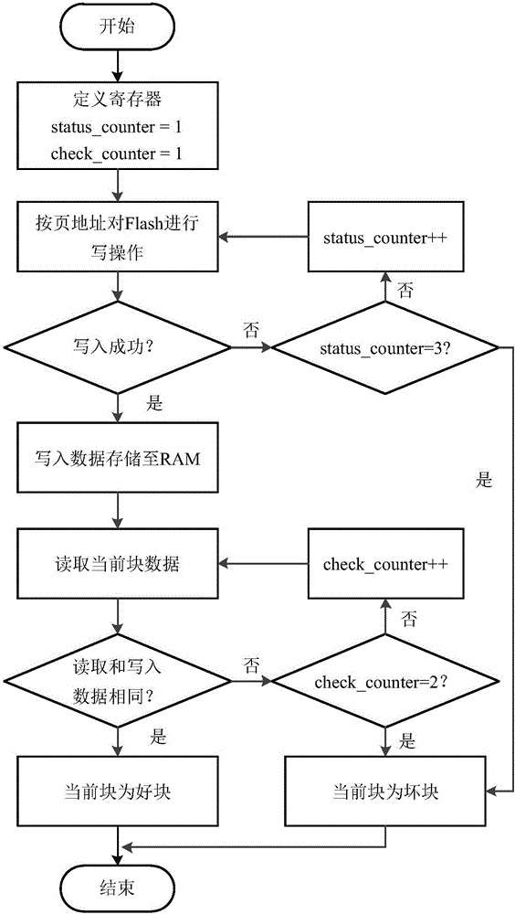
[0032] Such as figure 1 As shown, the Flash bad block detection process is as follows:

[0033] (1) Perform write operations on all blocks of the Flash chip according to the page address through the FPGA, and write one page at a time. After a write cycle is over, it is judged whether the writing is successful by checking the writing status flag bit. If the writing is not successful for 3 consecutive times, it is judged that the current block is a bad block;

[0034] (2) If the writing is successful, the writing data is stored in RAM. Read the content of the current block and compare it with the written data in RAM. If the content of reading and writing is different for two consecutive times, it is judged that the current block is a bad block;

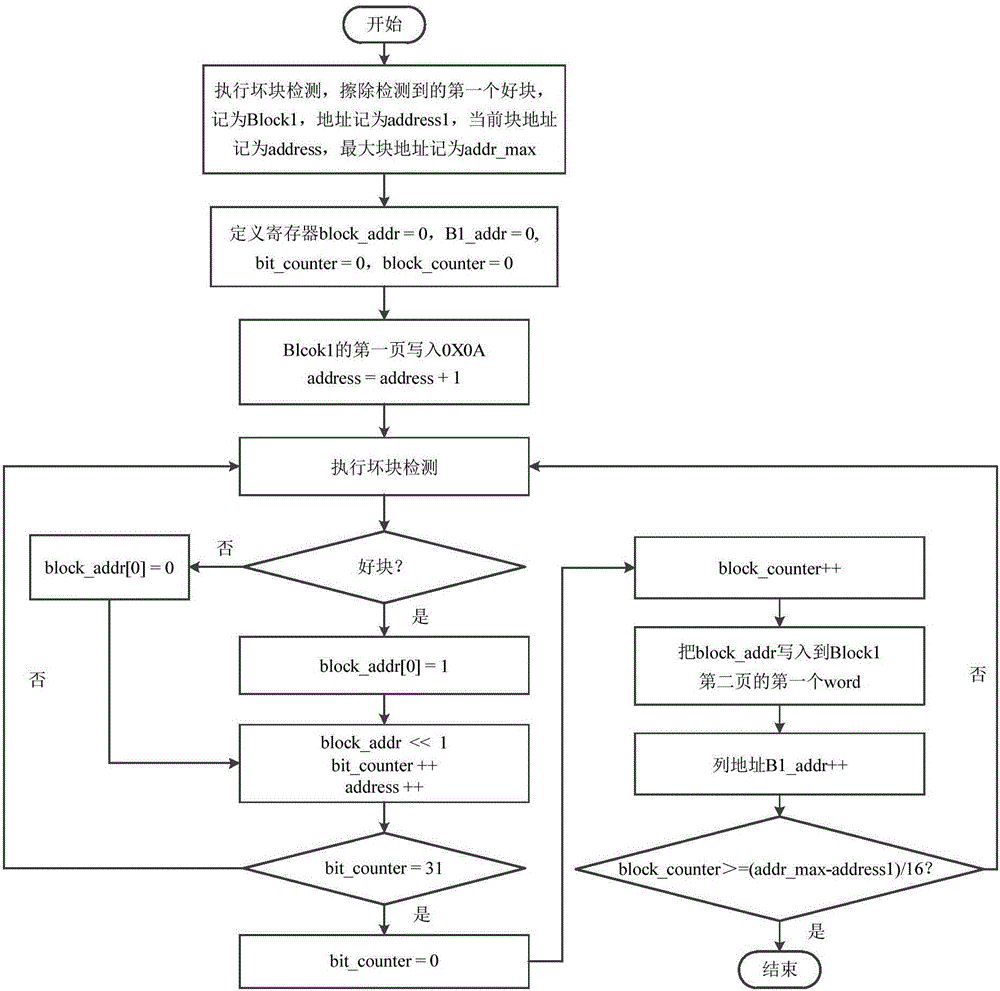
[0035] Such as figure 2 As shown, the bad block management process is as follows:

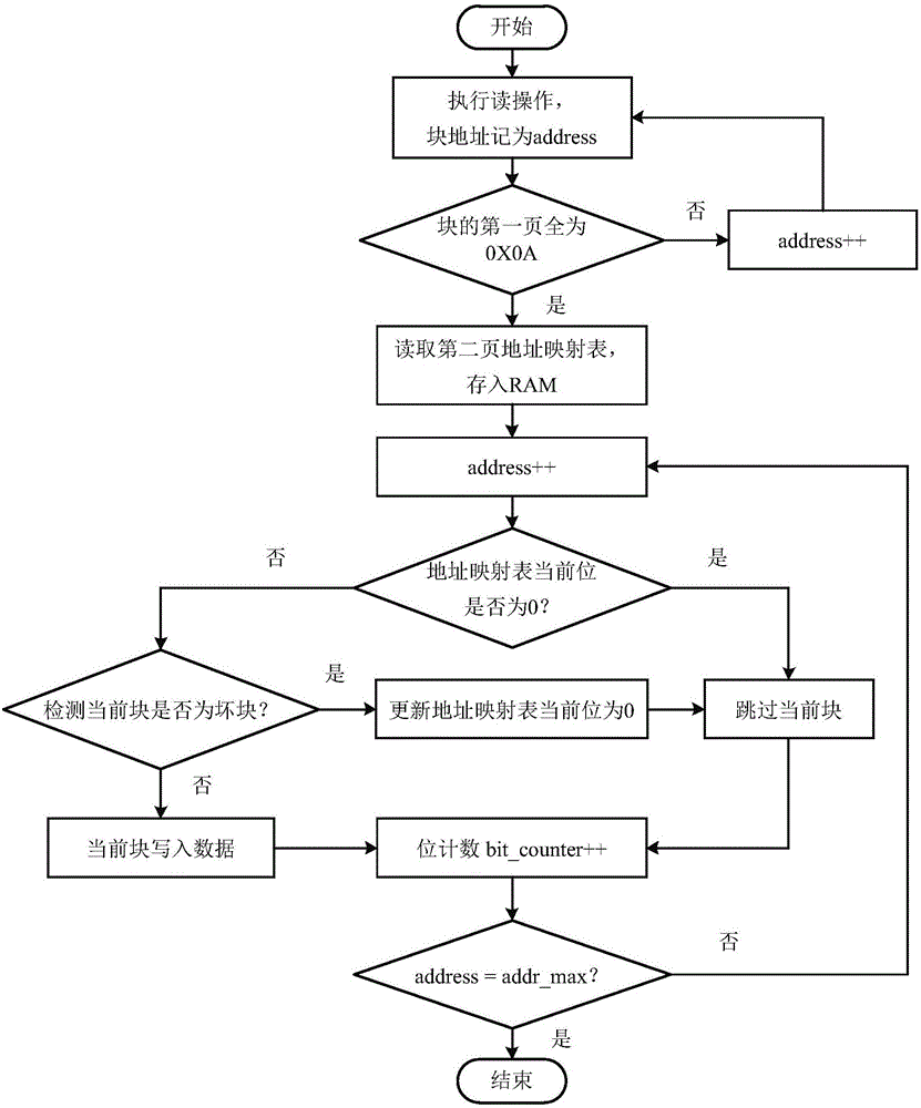
[0036] (1) Perform an erase operation...


PUM


Abstract

The invention discloses a NAND Flash fault-tolerance method based on a FPGA (Field Programmable Gate Array). The NAND Flash fault-tolerance method comprises the following steps: carrying out Flash bad block detection, bad block management and dynamic table lookup. The bad block is detected through judging whether the state of a Flash write zone bit is the same with read-write contents or not. The addresses of detected good blocks and bad blocks are managed by a bad block management algorithm, and an address mapping table is established. The FPGA carries out write, read and erasure operations on the Flash through a dynamic table lookup way, and the accuracy and the efficiency of data access are greatly improved. The method can directly improve the space use ratio of the Flash, the integral performance and the processing speed of the Flash can obtain an important guarantee, and the method has a reference meaning for the application development of the new-generation large-volume NAND Flash.

Description

technical field [0001] The invention relates to Flash fault-tolerant technology, in particular to an FPGA-based NAND Flash fault-tolerant method. Background technique [0002] With the continuous development of information technology, digital products have become a vital part of life. In the process of people's continuous pursuit of high-quality life, the capacity and processing performance of digital products such as smart phones, digital cameras, and players need to be improved urgently. At the same time, the storage industry is facing development opportunities brought about by huge demand. In today's civilian consumer electronics market, flash memory (Flash) plays a major role in non-volatile storage media. According to the difference in logic structure, it can be divided into NOR Flash and NAND Flash. NOR Flash occupies a dominant position in the early market. After technological innovation, NAND Flash emphasizes reducing the cost per bit. It can be easily upgraded th...

Claims


Application Information

Patent Timeline
IPC IPC(8): G06F12/02G06F12/06
CPCG06F12/0246G06F12/0646
Inventor 张晓峰史治国陈积明
Owner ZHEJIANG UNIV
Why Eureka
Try Eureka