Function traversal testing method for high performance SoC FPGA

A traversal test, high-performance technology, applied in the direction of measuring electricity, measuring devices, measuring electrical variables, etc., to achieve the effects of high test efficiency, strong portability, and strong versatility

Active Publication Date: 2016-08-17
FUDAN UNIV
View PDF4 Cites 27 Cited by
  • Summary
  • Abstract
  • Description
  • Claims
  • Application Information

AI Technical Summary

Problems solved by technology

[0004] While high-performance SoC-FPGA provides developers with great convenience, it also brings challenges to the function traversal test of each module resource.

Method used


Image

  • Function traversal testing method for high performance SoC FPGA
  • Function traversal testing method for high performance SoC FPGA
  • Function traversal testing method for high performance SoC FPGA

Examples


Embodiment Construction

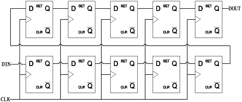
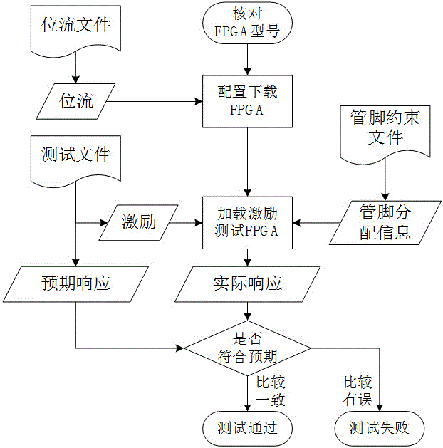
[0029] The implementation block diagram of the internal resource module function traversal test method of SoC FPGA is shown in Figure 1. The specific process is as follows:

[0030] First, design and generate bitstream files and pin constraint files for testing specified resources, and write test files (including test incentives and expected responses) according to the test methods of each resource module;

[0031] After checking the FPGA model, download the bit stream to the FPGA chip to complete the configuration of the FPGA;

[0032] Then, apply excitation signals to each port of FPGA according to the test file and pin constraint file, and read back the response signal of each output port of FPGA at the same time;

[0033] Finally, compare the actual response signal of the FPGA with the expected response signal in the test file. If they are consistent, the test is passed; otherwise, the test fails.

[0034] The result of software operation can be a graphical interface or ...


PUM


Abstract

The invention belongs to the technical field of integrated circuits, and relates to a function traversal testing method for high performance SoC FPGA. A set of complete function traversal testing method is established for CLB, BRAM, DSP, CM, IOB, clock network, interconnection and other resources in the high performance SoC FPGA, and corresponding bit stream is generated to apply excitation on an FPGA port and read back the response of the FPGA port. The response is compared with an expected result to realize the traversal covering test on the Soc FPGA resources. The test method is applicable to various high performance Soc FPGA with complex function and abundant resources and if of high application value in the FPGA test field. The test coverage rate and the test efficiency are high, the test cost is low, and the transferability and the universality are good.

Description

technical field [0001] The invention belongs to the technical field of integrated circuits, and in particular relates to a method for performing function traversal coverage tests on internal resource modules in high-performance SoC FPGA chips. Background technique [0002] Field Programmable Gate Array (Field Programmable Gate Array, FPGA) is a chip that can change its internal circuit logic function through programming. [0003] High-performance SoC (system on a programmable chip)-FPGA is the mainstream development trend of FPGA chips in recent years. It is characterized by programmable logic units (CLB: Configurable Logic Block) and programmable input and output units (IOB: Input Output Box) and interconnect resources, it also integrates block memory (BRAM), digital signal processor (DSP: Digital Signal Processing), clock manager (CM: clock managers) and other resources [1] , while retaining the customization flexibility of the FPGA itself, an efficient general-purpose i...

Claims


Application Information

Patent Timeline
Patent Type & Authority Applications(China)
IPC IPC(8): G01R31/3185
CPCG01R31/318519
Inventor 王健孙友志来金梅石超
Owner FUDAN UNIV
Why Eureka
Try Eureka