Unlock instant, AI-driven research and patent intelligence for your innovation.

Method for verifying I2C (Inter-Integrated Circuit) bus interface

A bus interface and interface technology, which is applied in the verification field of I2C bus interface in the FPGA verification stage, can solve the problems of FPGA port burnout and low clock bus, and achieve the effect of reducing chip tape-out costs and I2C function problems

Inactive Publication Date: 2016-08-17
CHIPSEA TECH SHENZHEN CO LTD
View PDF3 Cites 0 Cited by
  • Summary
  • Abstract
  • Description
  • Claims
  • Application Information

AI Technical Summary

Problems solved by technology

Assume that the I2C interface implemented by the tri-state INOUT port is directly used to communicate with the external standard I2C interface chip. At this time, the FPGA acts as the master device to read the data of the external slave device. If the FPGA communication clock is too fast, the slave device cannot respond. At this time The slave device will pull down the clock bus, and the FPGA as the master device does not know the status of the slave device at this time, and continues to force the output high level, which will cause the FPGA port to burn out

Method used


Image

  • Method for verifying I2C (Inter-Integrated Circuit) bus interface
  • Method for verifying I2C (Inter-Integrated Circuit) bus interface
  • Method for verifying I2C (Inter-Integrated Circuit) bus interface

Examples


Embodiment Construction

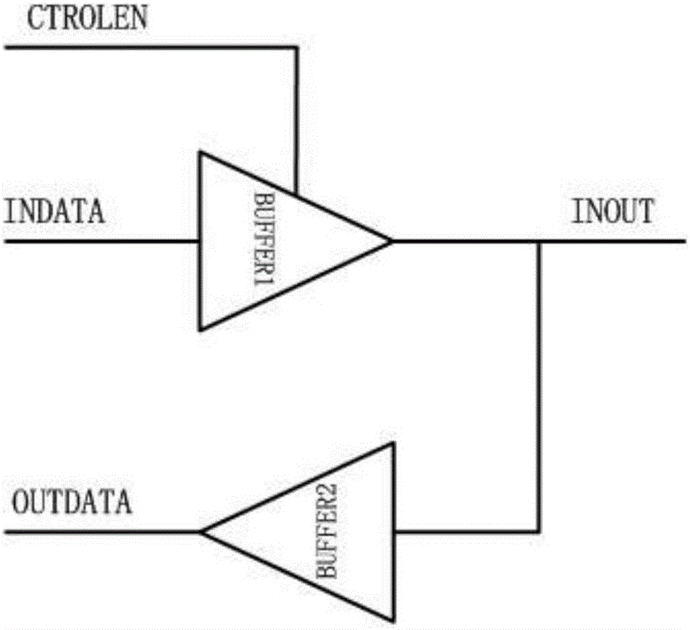
[0017] In order to make the object, technical solution and advantages of the present invention clearer, the present invention will be further described in detail below in conjunction with the accompanying drawings and embodiments. It should be understood that the specific embodiments described here are only used to explain the present invention, not to limit the present invention.

[0018] see image 3 As shown, the method for verifying the I2C bus interface realized by the present invention first decomposes the function of the tri-state port, and the tri-state port should make the port have both input and output functions, and then use the four-wire interface through the PNP triode, Imitate the open-drain structure of I2C to realize docking communication with external modules. The circuit that imitates the I2C open-drain structure is as follows image 3 shown. Before FPGA verification, the digital logic first decomposes the three-state port into a complete input function p...


PUM


Abstract

The invention discloses a method for verifying an I2C (Inter-Integrated Circuit) bus interface. The method comprises the following steps: firstly, decomposing the function of a tristate interface, wherein the tristate interface causes a port to own an input function and an output function; and then, through a PNP audion, utilizing a four-wire system interface to simulate the open interface structure of the I2C to realize connection communication with an external module. The complete verification of the I2C bus interface of a digital IC (Integrated Circuit) in a FPGA (Field Programmable Gate Array) verification stage can be realized, in addition, an I2C function problem after a chip is produced can be effectively reduced, and the tape-out cost of the chip is reduced.

Description

technical field [0001] The invention belongs to the technical field of the bus interface, in particular to the verification of the I2C bus interface in the FPGA verification stage. Background technique [0002] In chip design, in order to ensure that the various functions of the chip before tape-out meet the design requirements, and that there are no obvious mistakes in the chip manufactured at a high price, strict verification is often required in advance. Now the SOC or MCU products in the industry generally Composed of digital logic and analog circuits, the verification of digital logic and analog circuit functions can be simulated by software, digital logic can be verified by simulation software such as VSIM, modelsim, and analog circuit functions can be verified by candence software, but the software After all, the simulation is not a real environment, it can only verify the working conditions of the chip under ideal conditions, and there is still a big difference from ...

Claims


Application Information

Patent Timeline
IPC IPC(8): G06F11/22
CPCG06F11/221
Inventor 方学南
Owner CHIPSEA TECH SHENZHEN CO LTD