


Quick Research
Generate reliable direction feasibility study reports for your R&D in just a few steps.

Technical Q&A
Discover and master advanced knowledge NOW. Basics, ideas, possibilities, all at once.

Find Solutions
As an expert in R&D theories, this can generate solutions to your technical problems instantly.

Evaluate Feasibility
Analyze your overall solution with one click, know your potential R&D risks in advance.

Monitor Landscape
Get weekly tech updates, stay abreast of the latest tech innovations and key insights.
A PCB design method for an embedded system based on an A20
An embedded system and design method technology, applied in computing, special data processing applications, instruments, etc., can solve the problem of high manufacturing cost, and achieve the effect of reducing the number of PCB layers, ensuring stability, and reducing design and manufacturing costs
- Summary
- Abstract
- Description
- Claims
- Application Information
AI Technical Summary
Problems solved by technology
Method used
Image

Examples
specific Embodiment approach 1
[0015] 1, a kind of PCB design method based on the embedded system of A20, it is characterized in that concrete design method is as follows:
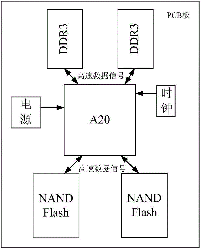
[0016] Design an embedded system based on A20, which mainly includes core controller A20, DDR3 (high-speed data cache), NAND Flash (mass data storage), clock chip and power module;
[0017] Such as figure 1 As shown, in the overall layout of the board, since DDR3 and NAND FLASH have many high-speed signal lines, DDR3 and NAND FLASH are respectively designed on the upper and lower sides or left and right sides of the core controller A20, and the Wiring is given priority; the power module and the clock chip are arranged on the left and right sides or the top and bottom sides of the core controller A20 respectively, and the clock chip is designed to be close to the core controller A20;
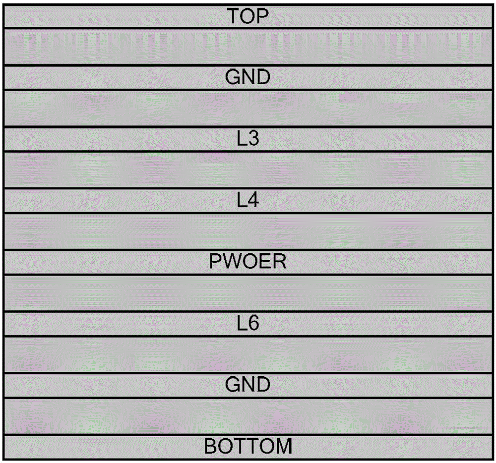
[0018] The PCB stackup design of the A20-based embedded system is 8 layers, including 5 wiring layers, 2 GND layers and 1 power layer.
[0019] image ...
specific Embodiment approach 2
[0020] The PCB laminate described in this embodiment is designed according to the following principles:
[0021] In terms of PCB stacking, priority is given to ensuring that the high-speed signal (above 100MHz) line has a complete reference ground plane, and the power signal is processed through the power plane as much as possible to ensure sufficient flow capacity. For low-speed signals (below 10MHz) or level signals, adjacent Layer routing to reduce the number of PCB layers and reduce costs.
[0022] Other steps and parameters are the same as those in Embodiment 1.
specific Embodiment approach 3
[0023] The specific design method of the PCB laminate described in this embodiment is as follows:
[0024] The PCB stack design is 8 layers, from top to bottom are TOP layer, GND layer, L3 layer, L4 layer, POWER layer, L6 layer, GND layer, BOTTOM layer;
[0025] DDR3 data lines and address lines have the highest rate, up to 1Gsps. Therefore, DDR3 is regarded as a single block in layout, and DDR3 is far away from NAND Flash, clock chip and power module design in plane layout, that is, DDR3 and NAND are combined in plane layout. The design of maximizing the distance between the Flash, the clock chip and the power module is to make the space as far as possible, and the ultimate goal is to ensure that the distance between the two signal lines is greater than 5 times the width of the PCB trace;
[0026] Prioritize the design of DDR3 wiring on the L3, L6, TOP, and BOTTOM layers, design the wiring length as short as possible, and the line spacing as large as possible; all data lines,...
PUM
 Abstract
Description
Claims
Application Information
 - R&D Engineer
- R&D Manager
- IP Professional
- Industry Leading Data Capabilities
- Powerful AI technology
- Patent DNA Extraction
Browse by: Latest US Patents, China's latest patents, Technical Efficacy Thesaurus, Application Domain, Technology Topic, Popular Technical Reports.
© 2024 PatSnap. All rights reserved.Legal|Privacy policy|Modern Slavery Act Transparency Statement|Sitemap|About US| Contact US: help@patsnap.com