PCB (printed circuit board)

A reference layer and link technology, applied in circuit devices, printed circuit components, high-frequency matchers, etc., can solve the problems of inconsistent signal transmission link impedance, signal integrity impact, etc.

Active Publication Date: 2016-08-17
LANGCHAO ELECTRONIC INFORMATION IND CO LTD
View PDF4 Cites 9 Cited by
  • Summary
  • Abstract
  • Description
  • Claims
  • Application Information

AI Technical Summary

Problems solved by technology

[0004] However, in the above technical solution, since the impedance of the coupling capacitor connected in series on the transmission line is usually smaller than the impedance of the transmission line, the i

Method used


Image

  • PCB (printed circuit board)
  • PCB (printed circuit board)
  • PCB (printed circuit board)

Examples


Embodiment Construction

[0039] In order to make the purpose, technical solutions and advantages of the embodiments of the present invention clearer, the technical solutions in the embodiments of the present invention will be clearly and completely described below in conjunction with the drawings in the embodiments of the present invention. Obviously, the described embodiments It is a part of the embodiments of the present invention, but not all of them. Based on the embodiments of the present invention, all other embodiments obtained by those of ordinary skill in the art without creative work belong to the protection of the present invention. scope.

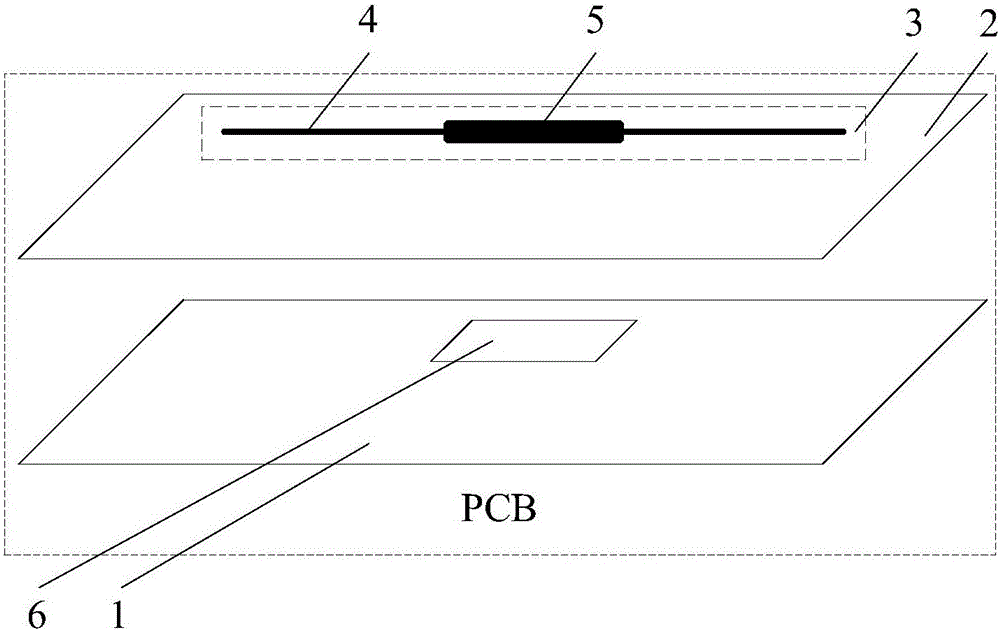
[0040] Such as figure 1 As shown, the embodiment of the present invention provides a PCB, including:

[0041] A first reference layer 1, a first medium layer 2, at least one signal transmission link 3, wherein the signal transmission link 3 is installed on the first side of the first medium layer 2, and the first reference layer 1 installed on the sec...


PUM


Abstract

The invention provides a PCB (printed circuit board). The PCB comprises a first reference layer, a first dielectric layer and at least one signal transmission link, wherein the corresponding signal transmission link is mounted on the first side of the first dielectric layer; the first reference layer is mounted on the second side of the first dielectric layer; each signal transmission link comprises two transmission lines and an alternating current (AC) coupling capacitor module, wherein the two transmission lines are connected through the AC coupling capacitor module; at least one impedance hole is formed in the first reference layer; the at least one impendence hole is in one-to-one correspondence with the corresponding AC coupling capacitor modules in the at least one signal transmission link; different impedance holes are not connected; and the open pore region of each impedance hole in the first reference layer comprises a projection region which is formed by the projection of the AC coupling capacitor module corresponding to the current impedance hole on the first reference layer in an orthographic projection manner. By adoption of the technical scheme, the signal completeness can be improved.

Description

technical field [0001] The present invention relates to the technical field of PCB (Printed Circuit Board, printed circuit board), in particular to a PCB. Background technique [0002] As the signal transmission rate continues to increase, the design requirements for the signal transmission link are also getting higher and higher, and the transmission link needs to have strong anti-interference ability to ensure the integrity of high-speed signals. [0003] At present, in order to ensure the integrity of high-speed signals, differential signal links are usually used to transmit high-speed signals sent from the signal transmitting device to the signal receiving device. At the same time, in order to prevent the direct voltage difference between the signal transmitting device and the signal receiving device from causing In case of a short circuit in the signal transmission link, signal sending device or signal receiving device, it is usually necessary to connect a coupling capa...

Claims


Application Information

Patent Timeline
IPC IPC(8): H05K1/02
CPCH05K1/0253
Inventor 刘强进李永翠
Owner LANGCHAO ELECTRONIC INFORMATION IND CO LTD
Why Eureka
Try Eureka