

Method and apparatus for detecting chip bonding conditions of printed circuit board
A printed circuit board and chip welding technology, which is applied in the direction of measuring devices, measuring electricity, and measuring electrical variables, etc., can solve the problems of damaged power supply, burned out power supply, low efficiency, etc., and achieve the effect of improving the product qualification rate
- Summary
- Abstract
- Description
- Claims
- Application Information
AI Technical Summary
Problems solved by technology
Method used
Image

Examples
Embodiment Construction
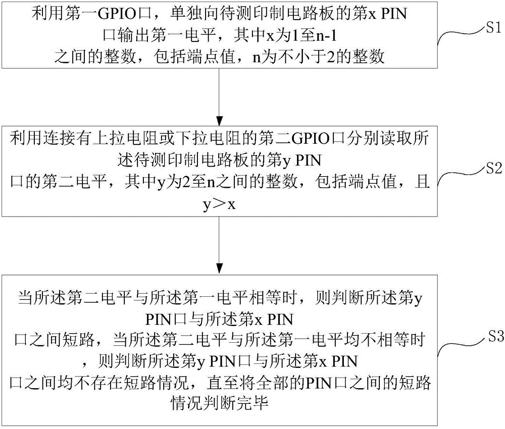
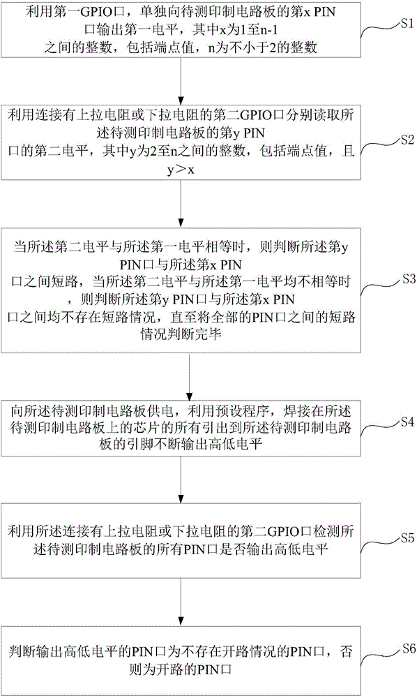
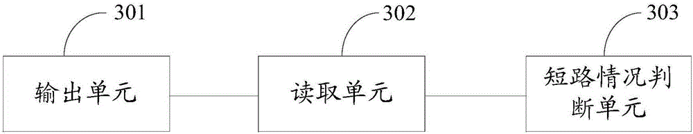
[0041] The core idea of the present invention is to provide a method and device for detecting the chip welding condition of a printed circuit board, which can quickly and non-destructively detect the chip welding condition of a printed circuit board, and locate the specific position where a short circuit occurs after the chip is welded, which is conducive to summary Reasons for insufficient soldering of printed circuit boards and improvement of product qualification rate.
[0042] The following will clearly and completely describe the technical solutions in the embodiments of the present invention with reference to the accompanying drawings in the embodiments of the present invention. Obviously, the described embodiments are only some, not all, embodiments of the present invention. Based on the embodiments of the present invention, all other embodiments obtained by persons of ordinary skill in the art without making creative efforts belong to the protection scope of the prese...
PUM
 Abstract
Description
Claims
Application Information