Complementary Cmos Structure And Method

A field-effect transistor and metal-oxide-semiconductor field-effect transistor technology, which is applied in the field of complementary metal-oxide-semiconductor field effect transistor structure and fabrication, can solve the problems of surface area and occupation of multiple integrated circuits.

Active Publication Date: 2016-08-24
TAIWAN SEMICON MFG CO LTD
View PDF6 Cites 7 Cited by
  • Summary
  • Abstract
  • Description
  • Claims
  • Application Information

AI Technical Summary

Problems solved by technology

To achieve this, separate n-channel and p-channel regions must be provided usin

Method used


Image

  • Complementary Cmos Structure And Method
  • Complementary Cmos Structure And Method
  • Complementary Cmos Structure And Method

Examples


Embodiment Construction

[0016] The making and using of this embodiment are discussed in detail below, however, it should be appreciated that the present invention provides practical innovative concepts which can be embodied in a wide variety of specific contexts. The specific examples discussed below are illustrative only and do not limit the scope of the invention.

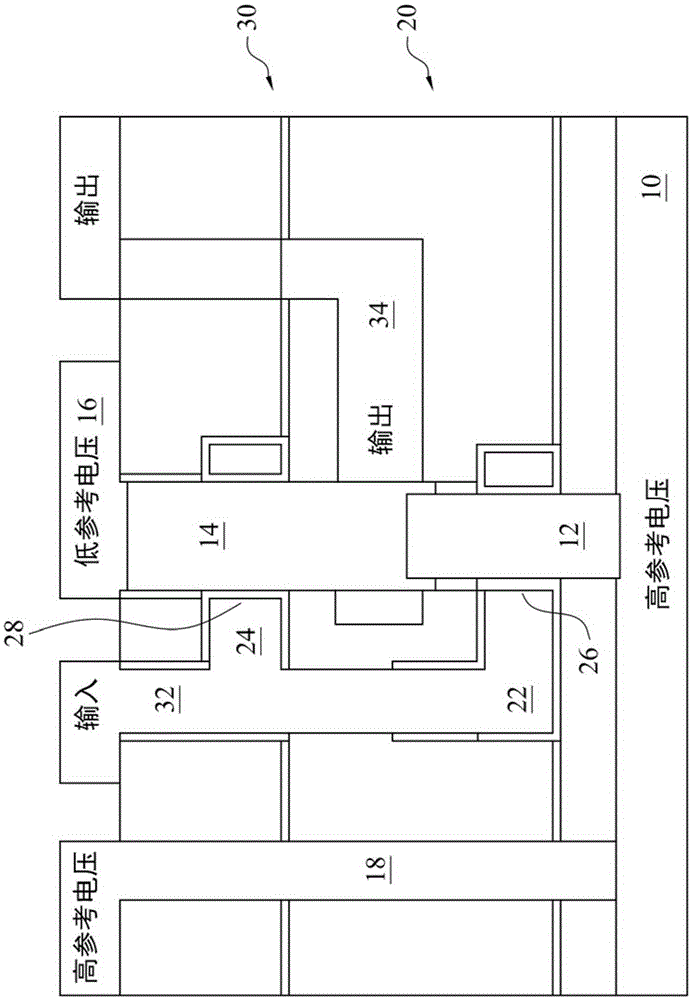
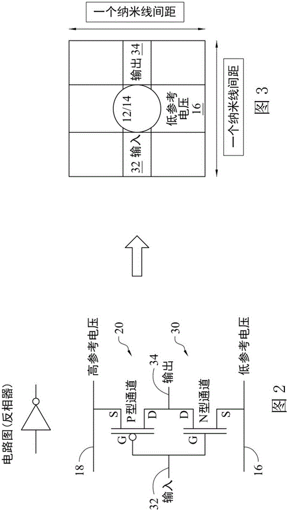
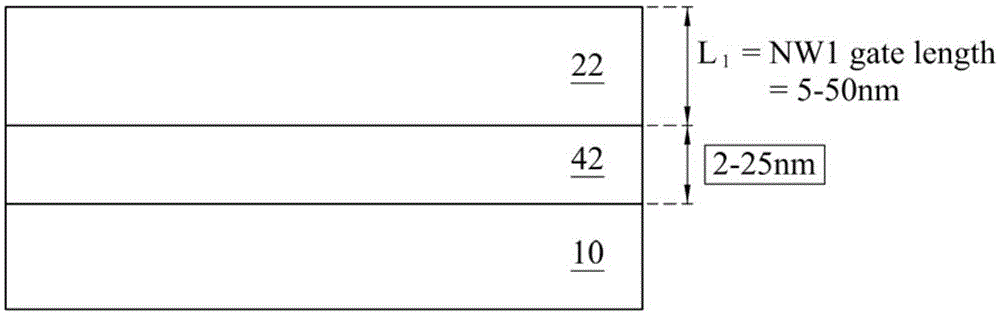
[0017] Embodiments of the present invention will be described below with specific content, that is, using stacked vertical surround (VGAA) or nanowire (NW) transistors as structures. Nevertheless, the innovative concepts of the present invention are not limited to the formation of specific structures. In fact, the innovative concept of the present invention can also be used for other structure formations. Furthermore, even though the present invention is directed to vertical wrap-around or nanowire circuit embodiments, the innovative concepts of the present invention can be applied to other types of integrated circuits, electronic stru...


PUM


Abstract

The invention discloses a complementary cmos structure and a method thereof. Selective deposition techniques are used to form a column having a lower portion that includes one type of semiconductor (e.g. germanium) and an upper portion of another type of semiconductor (e.g. indium arsenide. The lower portion of the column provides a channel region for a transistor of one type, while the upper column provides a channel region for a transistor of another type. This provides a complementary pair that occupies a minimum of integrated circuit surface area. The complementary transistors can be utilized in a variety of circuit configurations. Described are complementary transistors where the lower transistor is p-type and the upper transistor is n-type. The method is advantageous in that complementary transistors are provided, wherein the complementary transistors employ a minimum integrated circuit superficial area.

Description

technical field [0001] The present invention relates primarily to semiconductor device structures, and in certain embodiments, vertical complementary transistors and methods of stacking structures are provided. Background technique [0002] This has been an important goal in the invention of semiconductor fabrication in integrated circuits in order to fit more devices on integrated circuits. Higher circuit densities allow for higher performance devices and drastically reduce the cost of the underlying transistors. The traditional configuration of circuit components is to distribute horizontally on the surface of the semiconductor substrate. This provides ease and reduced complexity in manufacture. However, today's semiconductor design engineers are struggling with numerous limitations of horizontal devices. [0003] The biggest challenge is the limit of optical lithography. In photolithography, a layer of photosensitive material called photoresist is coated on the device...

Claims


Application Information

Patent Timeline
IPC IPC(8): H01L27/092H01L21/8238
CPCH01L21/8238H01L27/0922H01L27/0688H01L29/66742H01L21/0245H01L21/02639B82Y10/00B82Y40/00H01L29/26H01L29/267H01L29/42376H01L29/66469H01L29/068H01L27/092H01L21/8258H01L21/02381H01L21/02546H01L21/02603H01L21/823807H01L21/823871H01L21/823885H01L29/0649H01L29/0676H01L29/42392H01L29/78618H01L29/78642H01L29/78681H01L29/78684H01L29/78696H01L29/7827H01L29/16H01L29/20H01L29/1037H01L29/66666H01L21/02532H01L21/0262H01L21/02636H01L21/823828H01L21/823878
Inventor 理查·肯尼斯·奥克兰
Owner TAIWAN SEMICON MFG CO LTD
Why Eureka
Try Eureka