Semiconductor device and associated method of manufacture

A semiconductor and device technology, applied in the field of reduced surface field devices and trench Schottky diodes, can solve the problems of semiconductor devices that do not provide breakdown voltage performance

Active Publication Date: 2016-08-24
NEXPERIA BV
View PDF3 Cites 5 Cited by
  • Summary
  • Abstract
  • Description
  • Claims
  • Application Information

AI Technical Summary

Problems solved by technology

However, this approach may require additional photolithography and implantation steps and thus may not provide semiconductor devices capable of achieving the same breakdown voltage performance as trench terminated devices

Method used


Image

  • Semiconductor device and associated method of manufacture
  • Semiconductor device and associated method of manufacture
  • Semiconductor device and associated method of manufacture

Examples


Embodiment Construction

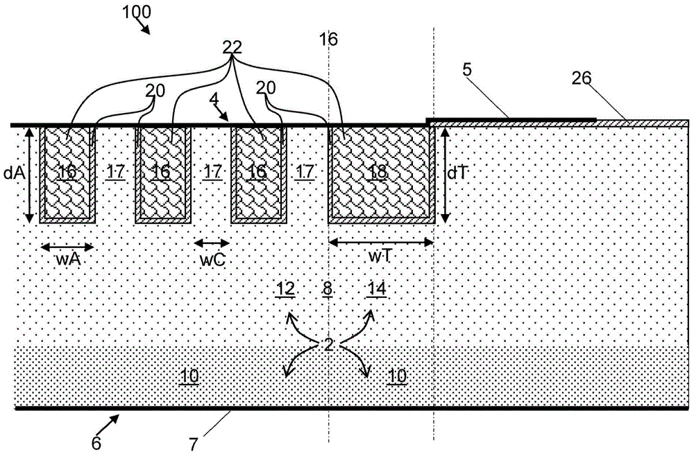
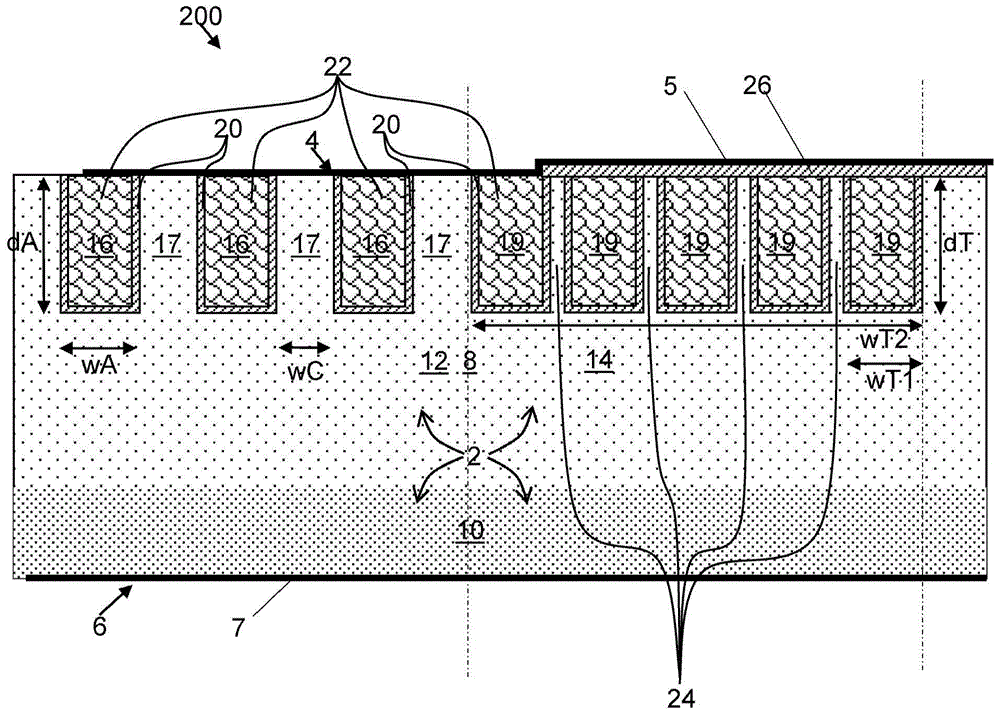
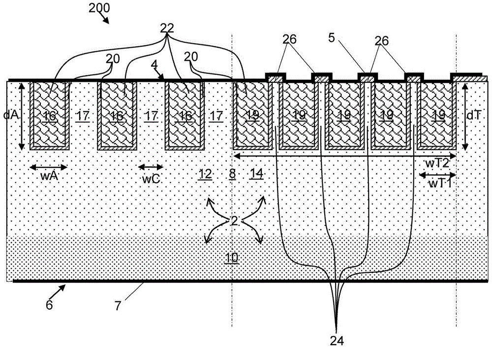
[0052] figure 1 A first semiconductor device 100 is shown. In general terms, device 100 uses a termination trench 18 that is wider than trench 16 in the active area of ​​the device. The width of the termination trench 18 can be designed such that field symmetry in the active area adjacent to the termination trench 18 can be ensured and so that the termination trench 18 can still be filled with polysilicon. The proposed termination design uses wider trenches in the termination region to ensure the symmetry of the electric field in the outermost mesa and prevent premature reverse bias breakdown during operation.

[0053] The device 100 comprises a body 2 having a first surface 4 and an opposite second surface 6 . The first semiconductor layer 8 is disposed in the body 2 and adjacent to the first surface 4 . The second semiconductor layer 10 is arranged adjacent to the second surface 6 . The first semiconductor layer 8 contains a drift region, and is an epitaxial layer that h...


PUM


Abstract

The disclosure relates to a semiconductor device comprising a body having: a first surface and an opposing second surface; a first semiconductor layer adjacent to the first surface; an active region comprising: a plurality of active trenches in the first surface, the plurality of active trenches extending from the first surface into the first semiconductor layer and having an active trench width, and a plurality of active cells, each active cell provided in the first semiconductor layer adjacent to an active trench, the active cells having an active cell width; and a termination region at a periphery of the first surface comprising: at least one termination trench, the at least one termination trench extending from the first surface into the first semiconductor layer, wherein the termination region has a width that is greater than the active trench width; and a number of termination trench separators having a width that is less than the active cell width, wherein the active trenches and the at least one termination trench each comprise a first insulator layer adjacent to the first semiconductor layer of the body, and wherein conductive material is disposed on the first insulating layer within each of the active trenches.

Description

technical field [0001] The present disclosure relates to semiconductor devices and associated fabrication methods. In particular, but not exclusively, the present disclosure relates to reduced surface field (RESURF) devices, such as trench Schottky diodes. Background technique [0002] Conventional reduced surface field (RESURF) semiconductor devices are fabricated on semiconductor substrates using epitaxial growth and implantation processes. Such devices may be vertical (where current flows through the device substantially perpendicular to the plane of the semiconductor substrate) or horizontal (where current flows through the substrate through the device). [0003] Typical examples of RESURF structures include diodes, transistors such as MOSFETs, or silicon controlled rectifiers with a region commonly called the drift region, which is depleted under reverse bias with a voltage much less than the breakdown voltage. A higher reverse bias voltage will result in a relatively...

Claims


Application Information

Patent Timeline
Patent Type & Authority Applications(China)
IPC IPC(8): H01L29/872H01L21/329H01L29/06
CPCH01L29/66143H01L29/8725H01L29/404H01L29/063H01L29/0696H01L29/407H01L21/67069
Inventor 提姆·伯切尔列扎·比塔什托马斯·伊格尔-霍兹恩多夫朱林佩
Owner NEXPERIA BV
Why Eureka
Try Eureka