
Optoelectronic device comprising light-emitting diodes

A technology of optoelectronic devices and light-emitting diodes, which is applied to circuits, electrical components, and electrical solid-state devices, and can solve problems such as increasing the manufacturing cost of optoelectronic systems

Active Publication Date: 2016-08-24
ALEDIA
View PDF5 Cites 14 Cited by
  • Summary
  • Abstract
  • Description
  • Claims
  • Application Information

AI Technical Summary

Problems solved by technology

These steps increase the manufacturing cost of the optoelectronic system

Method used


Image

  • Optoelectronic device comprising light-emitting diodes
  • Optoelectronic device comprising light-emitting diodes
  • Optoelectronic device comprising light-emitting diodes

Examples


Embodiment Construction

[0066] For the sake of clarity, in the various drawings, the same reference numerals are used to designate the same elements; moreover, as is common in the representation of electronic circuits, the various drawings are not drawn to scale. Furthermore, only elements useful for the understanding of the description are shown and described. Methods for controlling the optoelectronic devices described below are within the capabilities of those skilled in the art and are therefore not described again.

[0067] In the following description, the terms "substantially", "substantially" and "approximately" mean "within 10%" unless otherwise indicated. In addition, "a compound mainly formed of a material" or "a compound based on a material" means that the compound includes the material in a proportion greater than or equal to 95%, preferably, the proportion is greater than 99%.

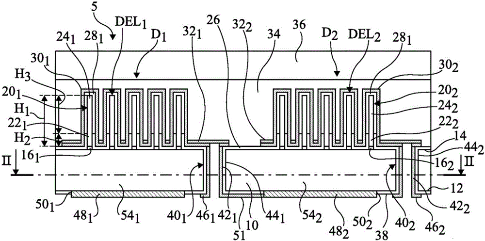
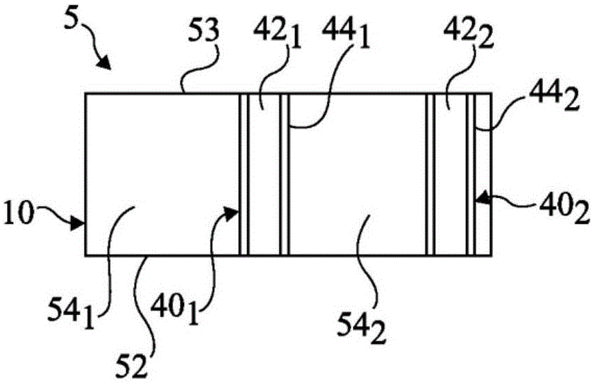
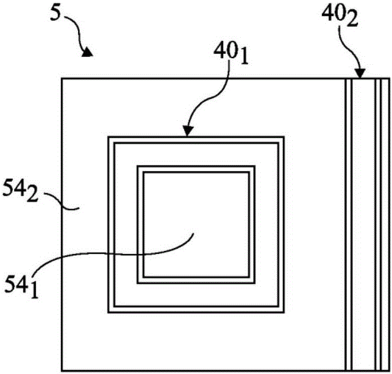
[0068] The present description relates to optoelectronic devices comprising three-dimensional elements such ...


PUM


Abstract

The invention relates to an optoelectronic device (5) comprising a semiconductor substrate (10) comprising first and second opposing faces (12, 14), a first set (D1) of first light-emitting diodes (DEL1) resting on a first portion (541) of the substrate and comprising conical or frustoconical wire-like semiconductor elements (201), a first electrode (301) covering each first light-emitting diode (DEL1), a first conductive portion (421) insulated from the substrate, extending through the substrate and connected to the first electrode; a second set (D2) of second light-emitting diodes (DEL2) resting on a second portion (542) of the substrate and comprising conical or frustoconical wire-like semiconductor elements (202), a second electrode (302 ) covering each second light-emitting diode (DEL2), a second conductive portion (422) insulated from the substrate and connected to the second electrode, and a first conductive element (461, 51, 482) connecting the first conductive portion to the second portion of the substrate on the side of the second face.

Description

[0001] Cross References to Related Applications [0002] This application claims priority from French patent application FR13 / 59409, which is hereby incorporated by reference. technical field [0003] The present invention relates to optoelectronic devices based on semiconductor materials and methods of manufacture thereof, in particular to optoelectronic devices comprising light-emitting diodes formed from three-dimensional elements, especially semiconductor microwires or nanowires. Background technique [0004] The phrase "optoelectronic device with light-emitting diodes" denotes a device capable of converting an electrical signal into electromagnetic radiation, in particular a device dedicated to emitting electromagnetic radiation, especially light. An example of a three-dimensional element capable of forming a light-emitting diode is a microwire or nanowire comprising a semiconductor material based on a compound mainly comprising at least one group III element and one gr...

Claims


Application Information

Patent Timeline
Patent Type & Authority Applications(China)
IPC IPC(8): H01L27/15H01L33/62H01L33/00H01L33/48
CPCH01L27/156H01L33/00H01L33/48H01L33/62H10K59/10H01L27/153H01L33/08H01L33/24H01L33/38H01L2924/12041H01L33/025H01L33/44H01L2933/0025H01L2933/0066
Inventor 克里斯多夫·布维尔埃尔文·多内尔
Owner ALEDIA
Learn More