Array substrate, preparation method therefor, and display device

A technology of an array substrate and a manufacturing method, which is applied in the display field, can solve problems such as reducing production efficiency and increasing production costs, and achieve the effects of improving production efficiency, improving performance, and simplifying the manufacturing process

Inactive Publication Date: 2016-09-07
BOE TECH GRP CO LTD
View PDF8 Cites 3 Cited by
  • Summary
  • Abstract
  • Description
  • Claims
  • Application Information

AI Technical Summary

Problems solved by technology

The array substrate of the existing ADSDS structure is provided with gate layer (comprising gate and gate line), gate insulating layer, active layer, source-drain electrode layer (comprising source electrode, drain ele

Method used


Image

  • Array substrate, preparation method therefor, and display device
  • Array substrate, preparation method therefor, and display device
  • Array substrate, preparation method therefor, and display device

Examples


Embodiment Construction

[0045] The following will clearly and completely describe the technical solutions in the embodiments of the present invention with reference to the accompanying drawings in the embodiments of the present invention. Obviously, the described embodiments are only some, not all, embodiments of the present invention. Based on the embodiments of the present invention, all other embodiments obtained by persons of ordinary skill in the art without making creative efforts belong to the protection scope of the present invention.

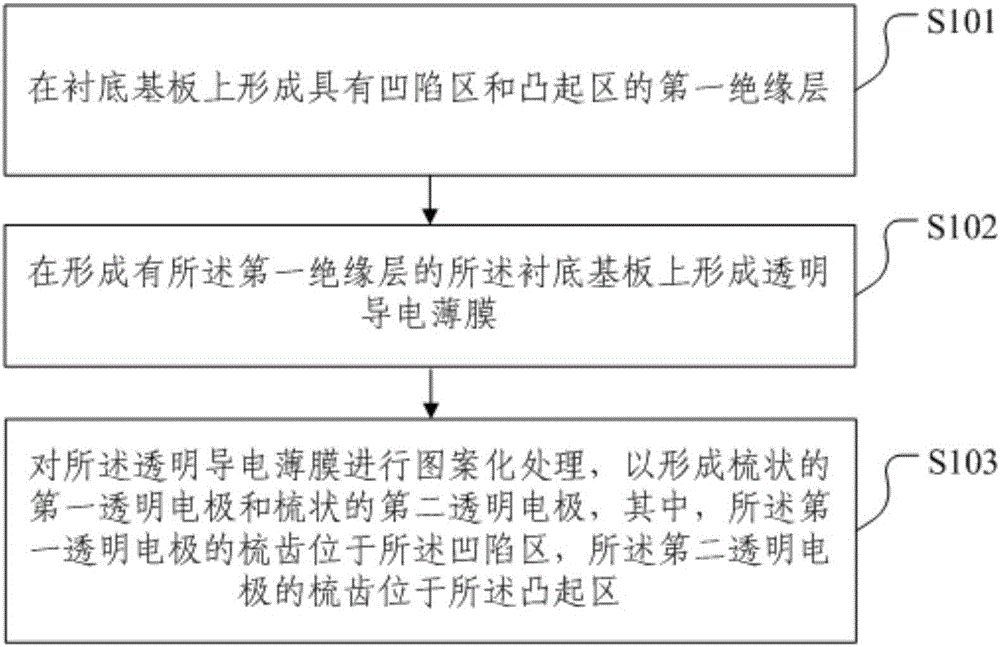
[0046] An embodiment of the present invention provides a method for manufacturing an array substrate. Such as figure 1 As shown, the production method includes the following steps:

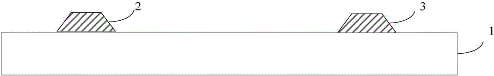
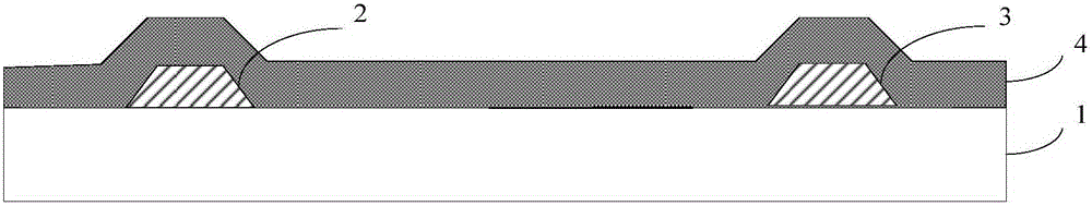
[0047] Step S101 , forming a first insulating layer having a recessed area and a raised area on a base substrate.

[0048] For example, an insulating film may be formed on the base substrate, and the insulating film may be patterned to form a first insulating layer having a rece...


PUM


Abstract

The invention relates to the technical field of display, and especially relates to an array substrate, a preparation method therefor, and a display device. The method comprises the following steps: forming a first insulating layer with a recessed region and a bulged region on a substrate; forming a transparent conductive film on the substrate with the first insulating layer; carrying out the patterning of the transparent conductive film, so as to form a first comb-shaped transparent electrode and a second comb-shaped transparent electrode, wherein the comb teeth of the first comb-shaped transparent electrode are located in the recessed region, and the comb teeth of the second comb-shaped transparent electrode are located in the bulged region. According to the invention, a pixel electrode and a common electrode are formed at the same time in the one-time patterning technology, and the method can reduce the number of patterning times, simplifies the manufacturing technology, reduces the production cost, and improves the production efficiency.

Description

technical field [0001] The present invention relates to the field of display technology, in particular to an array substrate, a manufacturing method thereof, and a display device. Background technique [0002] With the continuous development of display technology, thin film transistor liquid crystal display (Thin Film Transistor Liquid Crystal Display, TFT-LCD) occupies a dominant position in the field of flat panel display due to its advantages of small size, low power consumption, and no radiation. Among them, the Advanced super Dimension Switch (ADSDS) type TFT-LCD uses a horizontal electric field to drive liquid crystals, and is widely used because of its advantages of wide viewing angle, high aperture ratio, and high transmittance. The array substrate of the existing ADSDS structure is provided with gate layer (comprising gate and gate line), gate insulating layer, active layer, source-drain electrode layer (comprising source electrode, drain electrode and data line), p...

Claims


Application Information

Patent Timeline
IPC IPC(8): H01L21/77H01L27/12G02F1/1343
CPCH01L27/127G02F1/134309G02F2201/121G02F2201/123H01L27/1214H01L27/124
Inventor 姚琪曹占锋张锋
Owner BOE TECH GRP CO LTD
Why Eureka
Try Eureka