A kind of emi automatic adjustment device and emi automatic adjustment method

A technology for automatically adjusting devices and configuring information, applied in automatic power control, electrical components, etc., can solve problems affecting chip performance and achieve the effect of solving EMI problems

Active Publication Date: 2018-11-20
FUZHOU ROCKCHIP SEMICON
View PDF3 Cites 0 Cited by
  • Summary
  • Abstract
  • Description
  • Claims
  • Application Information

AI Technical Summary

Problems solved by technology

But in the current technology, usually by changing the frequency or forcibly increasing the jitter (clock jitter) of the clock to transfer or lower the spectrum energy of the clock, but this kind of disadvantage is also obvious, changing the frequency will affect the performance of the chip, Especially some circuits sensitive to frequency, such as some communication interface circuits
Then forcibly increasing the jitter of the clock can level the spectrum energy and reduce it, but the degradation of the clock quality will also obviously have a negative impact on the circuit performance, and this impact exists at all frequencies

Method used


Image

  • A kind of emi automatic adjustment device and emi automatic adjustment method

Examples


Embodiment Construction

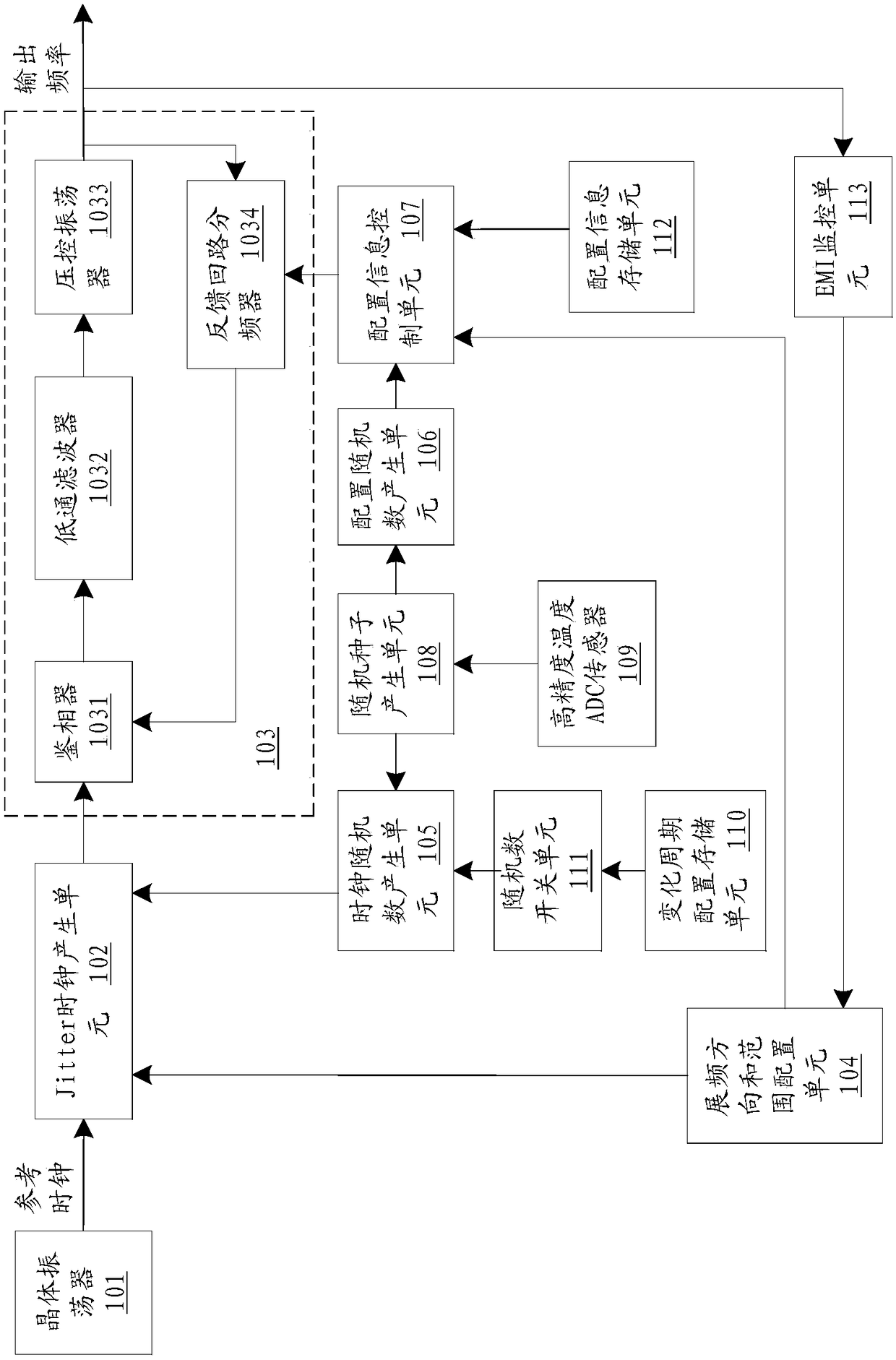
[0049] see figure 1As shown, the EMI automatic adjustment device of the present invention includes a crystal oscillator 101, a jitter clock generation unit 102, a PLL circuit 103, a spread spectrum direction and range configuration unit 104, a clock random number generation unit 105, a configuration random number generation unit 106, a configuration an information control unit 107, a random seed generation unit 108, a high-precision temperature ADC sensor 109, a change period configuration storage unit 110, a random number switch unit 111, a configuration information storage unit 112, and an EMI monitoring unit 113;

[0050] The crystal oscillator 101, the jitter clock generating unit 102, and the PLL circuit 103 are connected in sequence;

[0051] The spread spectrum direction and range configuration unit 104 is respectively connected to the jitter clock generation unit 102 and the configuration information control unit 107;

[0052] The random seed generating unit 108 is re...


PUM


Abstract

The present invention provides an EMI automatic adjustment device and an EMI automatic adjustment method. The EMI automatic adjustment device comprises a crystal oscillator, a jitter clock generation unit, a PLL circuit, a spectrum spreading direction and scope configuration unit, a clock random number generation unit, a configuration random number generation unit, a configuration information control unit, a random seed generation unit, a high precision temperature ADC sensor, a change cycle configuration storage unit, a random number switch unit, a configuration information storage unit, and an EMI monitoring unit. EMI is automatically checked, or the spectrum spreading processing of PLL is carried out according to a configured EMI frequency point, the spectrum spreading operation of a clock is carried out through a configurable frequency spreading direction, thus original spectral energy spike is flattened, and an EMI problem is solved.

Description

technical field [0001] The invention relates to a chip design, in particular to an EMI automatic adjustment device for a chip and an EMI automatic adjustment method. Background technique [0002] EMI (Electromagnetic Interference, Electromagnetic Interference) refers to the interference source coupling (interference) its signal to another electrical network through the medium. In chip design, high-speed PCB and system design, high-frequency signal lines, integrated circuit traces and pins, various types of connectors, etc. may become sources of interference, affecting the normal operation of other systems or other subsystems in the system. [0003] As the operating frequency of SOC chips becomes higher and higher, EMI has become an important factor affecting chip performance. However, in the current technology, the spectral energy of the clock is usually transferred or pulled down by changing the frequency or forcibly increasing the jitter (clock jitter) of the clock. Howev...

Claims


Application Information

Patent Timeline
Patent Type & Authority Patents(China)
IPC IPC(8): H03L7/085H03L7/18
CPCH03L7/085H03L7/18
Inventor 廖裕民黄一凡
Owner FUZHOU ROCKCHIP SEMICON
Why Eureka
Try Eureka