Photoelectric detector based on graphene planar junction

A photodetector and graphene technology, applied in the field of photodetection, can solve problems such as large dark current, unfavorable photodetector application development, and low efficiency, so as to improve photoresponsivity, avoid graphene chemical doping process, The effect of simple structure

Active Publication Date: 2016-09-21
CHONGQING INST OF GREEN & INTELLIGENT TECH CHINESE ACADEMY OF SCI
View PDF6 Cites 10 Cited by
  • Summary
  • Abstract
  • Description
  • Claims
  • Application Information

AI Technical Summary

Problems solved by technology

However, currently observed photothermoelectric phenomena are mainly based on monolayer-bilayer graphene interfaces (see Xu X.D. et al., “Photo-Thermoelectric Effect at a Graphene Interface Junction”, Nano Letters, 10, 562, 2010), top-gate back In complex structures such as dual-gate devices with simultaneous gate modulation (see Gabor N.M.et al., "Hot Carrier–Assisted Intrinsic Photoresponse in Graphene", Science, 4,334,2011), it is not conducive to the application and development of photodetectors
[0005] In general, the special energy band structure of graphene makes it a promising photodetector material, but the current graphene photodetector structure generally has problems such as large dark current and low efficiency. A simple process , the photothermoelectric graphene photodetector structure with practical process operability has great potential demand

Method used


Image

  • Photoelectric detector based on graphene planar junction
  • Photoelectric detector based on graphene planar junction
  • Photoelectric detector based on graphene planar junction

Examples


Embodiment Construction

[0039] Embodiments of the present invention are described below through specific examples, and those skilled in the art can easily understand other advantages and effects of the present invention from the content disclosed in this specification. The present invention can also be implemented or applied through other different specific implementation modes, and various modifications or changes can be made to the details in this specification based on different viewpoints and applications without departing from the spirit of the present invention.

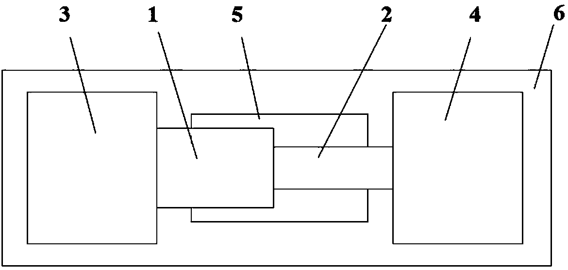
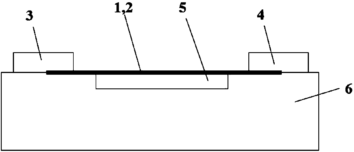
[0040] The graphene planar junction type photodetector that the present invention proposes in detail below in conjunction with accompanying drawing, as Figure 2-4 shown. The main process steps include:

[0041] 1. The substrate 6 is prepared. The substrate 6 is an insulating substrate or a non-insulating substrate with an insulating layer. In this embodiment, a heavily doped P-type silicon substrate covered with thermally oxidized...


PUM


Abstract

The invention provides a photoelectric detector based on graphene planar junction. The photoelectric detector based on graphene planar junction comprises a substrate, two ends of the substrate surface are respectively provided with a metal electrode, a graphene integral band is connected between the metal electrodes, one end of the graphene integral band is a wide band part, and the other end of the graphene integral band is a narrow band part. For the graphene planar junction type photoelectric detector provided by the invention, difference of seebeck coefficients of wide and narrow bands is caused by means of difference of graphene band energy band structures of different width, and thus, zero-bias photoelectric detection is realized based on optical thermo-electric effect. Device structures and technical processes in the invention are simple, a lengthy graphene chemical doping technology is avoided, and a parallel structure can be realized for improving optical responsivity; based on the infrared absorption characteristics of graphene, the photoelectric detector provided by the invention can be used for mid and far-infrared and terahertz photoelectric detection, and is a very practical photoelectric detector structure.

Description

technical field [0001] The invention belongs to the technical field of photoelectric detection and relates to a photoelectric detector based on graphene planar junctions. Background technique [0002] Graphene is an emerging two-dimensional atomic crystal material. Its ultra-wide light absorption band and ultra-fast carrier mobility, as well as its compatibility with silicon-based integrated circuit technology, make graphene materials especially suitable for photodetection. device making. At present, photodetectors based on graphene materials have made remarkable progress in broadband detection and ultrafast photodetectors. [0003] Currently, graphene-based photodetectors are mainly based on photoconductive, built-in field photovoltaic, photopyroelectric, and bolometric types (see Koppens F.H.L. et al., “Photodetectors based on graphene, other two-dimensional materials and hybrid systems”, Nature Nanotechnology, 9, 780, 2014). The photoconductive graphene photodetector m...

Claims


Application Information

Patent Timeline
Patent Type & Authority Applications(China)
IPC IPC(8): H01L35/28H01L35/32H01L35/22H01L35/34
CPCH10N10/855H10N10/10H10N10/01H10N10/17
Inventor 申钧魏兴战冯双龙魏大鹏杨俊周大华史浩飞杜春雷
Owner CHONGQING INST OF GREEN & INTELLIGENT TECH CHINESE ACADEMY OF SCI
Why Eureka
Try Eureka