Broadband photoelectric detector based on graphene homojunction and preparation method of broadband photoelectric detector

A photodetector and graphene technology, applied in the field of photoelectric detection, can solve the problems of slow response time, uncontrollability, high responsivity of graphene photodetector, etc., achieve high mobility and improve separation efficiency

Active Publication Date: 2021-10-01
CHONGQING INST OF GREEN & INTELLIGENT TECH CHINESE ACADEMY OF SCI +1
View PDF6 Cites 1 Cited by
  • Summary
  • Abstract
  • Description
  • Claims
  • Application Information

AI Technical Summary

Problems solved by technology

Graphene photodetectors lacking a gain mechanism cannot achieve high responsivity
[0004] Recent studies have shown that graphene composite photodetectors use the trap effect to provide a gain mechanism to achieve high responsivity (see Fang, Hehai; Hu, Weida. Photogating in Low Dimensional Photodetectors. Advanced Science, 2017, 4(12): 1700323.), however light absorption depends on semiconductor materials rather than graphene, so the absorption spectrum is limited to a narrow fixed band of light-absorbing materials
The interface contact problem has always been a challenge for heterojunction devices. Interface defects can lead to slow response time and uncontrollable defects.
These have limited the further development of high-gain photodetectors

Method used


Image

  • Broadband photoelectric detector based on graphene homojunction and preparation method of broadband photoelectric detector
  • Broadband photoelectric detector based on graphene homojunction and preparation method of broadband photoelectric detector
  • Broadband photoelectric detector based on graphene homojunction and preparation method of broadband photoelectric detector

Examples


Embodiment 1

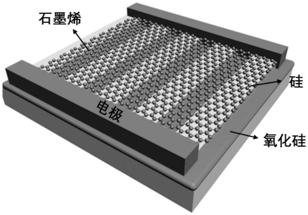
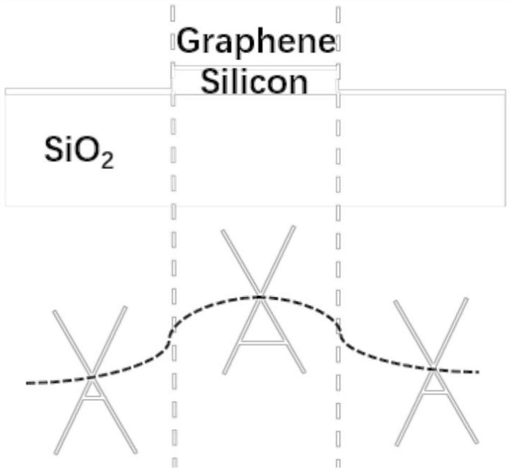
[0035] This embodiment is a broadband photodetector based on graphene homojunction. The structure of the photodetector includes an SOI substrate, graphene strips and electrodes, the graphene strips are covered on the substrate, the SOI substrate includes silicon and silicon oxide, and the two electrodes are connected by the graphene strips and arranged separately There are two metal electrodes above the two ends of the graphene strip, and there are periodically parallel channels on the substrate surface, such as figure 1 shown.

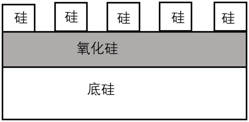
[0036] From top to bottom, the substrate includes doped top silicon with a thickness of 220nm, silicon oxide with a thickness of 2μm, and lightly doped bottom silicon with a thickness of 450μm. The surface of the substrate is divided into a lightly doped top silicon region and a silicon oxide region. These two regions Periodically alternately arranged in parallel to form a channel, the arrangement periods are 300nm, 600nm, 800nm, 1200nm, 3μm and 10μm...

Embodiment 2

[0044] This embodiment is a preparation method of a broadband photodetector based on a graphene homojunction, and its preparation process is substrate preparation, substrate etching, graphene growth, graphene transfer, metal electrode preparation, and graphene striping ,Such as Figure 4 shown.

[0045] Substrate preparation, in this embodiment, the structure from top to bottom is lightly doped top silicon with a thickness of 220 nm, silicon oxide with a thickness of 2 μm, and a lightly doped bottom silicon SOI substrate with a thickness of 450 μm. Before use, the substrate was cleaned by ultrasonication with acetone and ethanol for 20 min.

[0046] For substrate etching, 475PMMA is used as photoresist, and electron beam direct writing is used as exposure method to write grating patterns of different periods on the top silicon surface. A 30nm chromium layer is evaporated on the substrate surface, and the top silicon layer in the unexposed area is exposed after peeling off, a...


PUM

PropertyMeasurementUnit
thicknessaaaaaaaaaa
thicknessaaaaaaaaaa
thicknessaaaaaaaaaa

Abstract

The invention discloses a broadband photoelectric detector based on a graphene homojunction and a preparation method of the broadband photoelectric detector. The detector comprises a substrate, a graphene strip and electrodes, wherein the graphene strip covers the substrate, the electrodes are two metal electrodes respectively arranged above two ends of the graphene strip, and the surface of the substrate comprises channels which are periodically arranged in parallel. The preparation method comprises the following steps: etching a silicon-silicon oxide-silicon substrate to form the periodic parallel channels; preparing a graphene film and transferring the graphene film to the substrate; then respectively depositing metals at two ends of the graphene film to form the metal electrodes; and finally striping the graphene film. According to the broadband photoelectric detector, the defect that the service life of graphene carriers is short in the prior art is overcome, the broadband spectrum detection capacity of graphene is excited, middle-infrared band detection can be carried out without dependence on optical assistance, and the broadband photoelectric detector is an extremely practical photoelectric detector structure.

Description

technical field [0001] The invention relates to the technical field of photoelectric detection, in particular to a graphene homojunction-based broadband photodetector and a preparation method thereof. Background technique [0002] Graphene is a very attractive material for broadband light detection in hyperspectral imaging and sensing systems due to its zero bandgap, with absorption ranging from ultraviolet to far infrared. [0003] However, the low light absorption rate (2.3%) and short carrier lifetime (1 ps) of graphene lead to the extremely low quantum efficiency of graphene, which has been a challenge for its application in optoelectronic devices. The quantum efficiency of photodetectors using graphene itself as a light-absorbing material is very low. Patent 201510825269.8 "Photodetectors based on graphene thin films and their preparation methods" discloses a photovoltaic graphene photodetector based on graphene back-gate transistors , using the built-in electric field...

Claims


Application Information

Patent Timeline
Patent Type & Authority Applications(China)
IPC IPC(8): H01L31/103H01L31/0224H01L31/0352H01L31/18
CPCH01L31/103H01L31/022408H01L31/0352H01L31/1804Y02P70/50
Inventor 伍俊魏兴战蒋昊史浩飞韩钦申钧
Owner CHONGQING INST OF GREEN & INTELLIGENT TECH CHINESE ACADEMY OF SCI
Why Eureka
Try Eureka