Silicon carbide power device terminal structure and manufacturing method thereof

A technology of power devices and terminal structures, which is applied in semiconductor/solid-state device manufacturing, semiconductor devices, electrical components, etc., to achieve the effects of smooth electric field distribution, reduced electric field concentration, and reduced sensitivity

Active Publication Date: 2019-06-04
杰平方半导体(上海)有限公司
View PDF6 Cites 0 Cited by
  • Summary
  • Abstract
  • Description
  • Claims
  • Application Information

AI Technical Summary

Problems solved by technology

Traditional silicon devices are limited by the characteristics of the material itself, getting closer and closer to its theoretical limit

Method used


Image

  • Silicon carbide power device terminal structure and manufacturing method thereof
  • Silicon carbide power device terminal structure and manufacturing method thereof
  • Silicon carbide power device terminal structure and manufacturing method thereof

Examples


Embodiment Construction

[0039] The following describes the implementation of the present invention through specific specific examples. Those skilled in the art can easily understand other advantages and effects of the present invention from the content disclosed in this specification. The present invention can also be implemented or applied through other different specific embodiments, and various details in this specification can also be modified or changed based on different viewpoints and applications without departing from the spirit of the present invention.

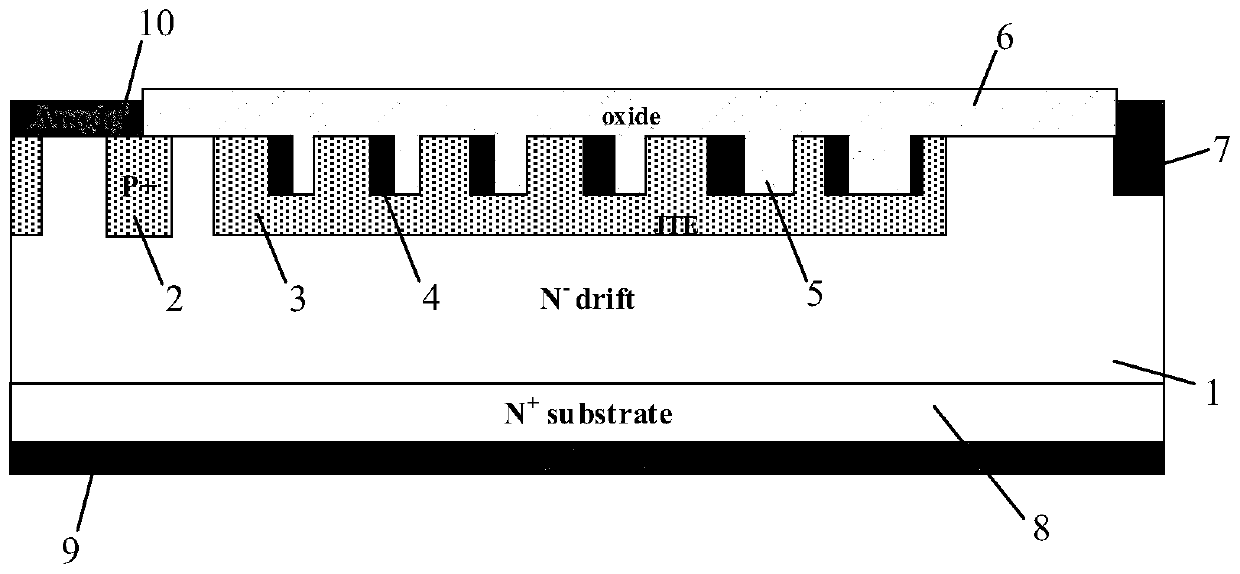
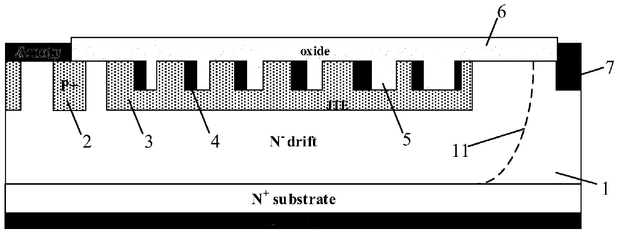
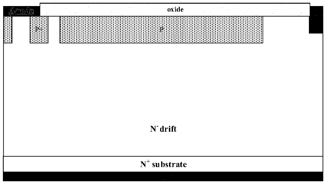
[0040] A silicon carbide power device terminal structure, including a device cell and a device terminal;

[0041] The device cell is a traditional junction barrier control Schottky structure, that is, there are several interphase heavily doped P-type body regions 2 connected to the anode metal 10 on the N-drift region 1;

[0042] The device terminal is located in the N-drift region 1 on the N-type heavily doped substrate 8 and includes a P-type j...


PUM

PropertyMeasurementUnit
thicknessaaaaaaaaaa

Abstract

The invention provides a silicon carbide power device terminal structure and a manufacturing method thereof. The device includes a device cell and a device terminal; the device terminal includes a P-type junction terminal expansion area, and an N+ injection ring and an etching ring are located in the P-type junction terminal expansion area. The groove, the etched groove is connected to the N+ injection ring, the etched groove is located outside the N+ injection ring, the inside of the etched groove is filled with an oxide layer, and the adjacent N+ injection ring is expanded by the etched groove and the P-type junction terminal The adjacent etched grooves are separated by the P-type junction terminal expansion area and the N+ injection ring, and the upper surfaces of the P-type junction terminal expansion area and the N+ injection ring are covered with an oxide layer. The present invention makes the electric field distribution tend to be gentle, so that The depletion layer in the terminal area is fully expanded, which improves the withstand voltage capability of the terminal and reduces the sensitivity of the breakdown voltage of the device to the concentration of the JTE area. The structure of the invention can effectively reduce the local electric field on the device surface, reduce the impact ionization rate on the device surface at the same time, reduce the surface leakage and improve the reliability of the device surface.

Description

Technical field [0001] The invention belongs to the technical field of semiconductor power devices. In particular, it is a silicon carbide power device terminal structure and a manufacturing method thereof. Background technique [0002] With the development of modern technology and the improvement of people's living standards, people continue to put forward higher requirements for semiconductor power devices in terms of their volume, reliability, withstand voltage, and power consumption. Traditional silicon devices are limited by the characteristics of the material itself and are getting closer to its theoretical limit. In this context, people began to explore new materials other than silicon materials, and silicon carbide technology was born. Silicon carbide has a series of advantages that traditional silicon materials do not have, such as higher breakdown electric field, higher thermal conductivity, and larger band gap, making silicon carbide more suitable for high-voltage po...

Claims


Application Information

Patent Timeline
Patent Type & Authority Patents(China)
IPC IPC(8): H01L29/872H01L29/06H01L21/329
CPCH01L29/0619H01L29/6606H01L29/872
Inventor 邓小川柏思宇宋凌云陈茜茜张波
Owner 杰平方半导体(上海)有限公司
Why Eureka
Try Eureka