Transverse high-pressure device for reducing hot carrier effect

A lateral high voltage, hot carrier technology, used in semiconductor devices, electrical components, circuits, etc., to reduce carrier temperature and impact ionization rate, prolong service life, and inhibit injection into the oxide layer.

Inactive Publication Date: 2015-05-06
UNIV OF ELECTRONICS SCI & TECH OF CHINA
View PDF5 Cites 0 Cited by
  • Summary
  • Abstract
  • Description
  • Claims
  • Application Information

AI Technical Summary

Problems solved by technology

However, the hot-carrier injection effect of lateral high-voltage devices not only occurs at the end of the channel, but also has serious hot-carrier effects in the drift region.

Method used


Image

  • Transverse high-pressure device for reducing hot carrier effect
  • Transverse high-pressure device for reducing hot carrier effect
  • Transverse high-pressure device for reducing hot carrier effect

Examples


Embodiment 1

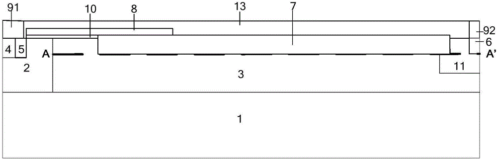
[0030] A lateral high-voltage device with reduced hot-carrier effects, such as figure 2 As shown, it includes a second conductivity type semiconductor substrate 1; a first conductivity type body region 2 and a second conductivity type well region 3 formed on the second conductivity type semiconductor substrate 1; The first conductivity type contact region 4 and the first conductivity type source region 5 in the first conductivity type; the shallow trench isolation region 7 and the first conductivity type buffer region 11 formed in the second conductivity type well region 3, the shallow trench isolation region 7 is located in the second conductivity type well region 3 Between the first conductivity type body region 2 and the first conductivity type buffer region 11; the second conductivity type drain region 6 formed in the first conductivity type buffer region 11; formed in the first conductivity type source region 5 and the shallow trench isolation region The gate oxide layer...

Embodiment 2

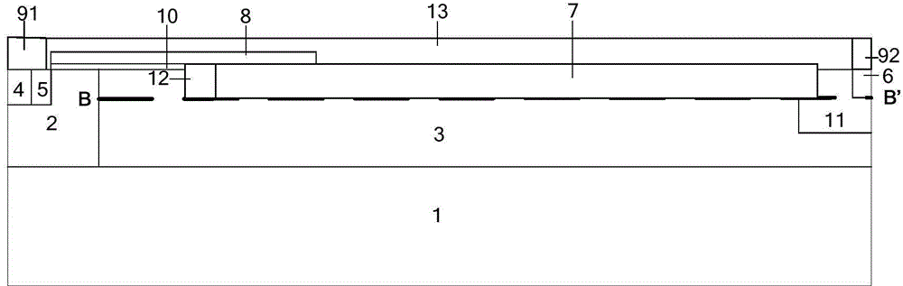
[0036] Such as image 3 As shown, the difference between the lateral high voltage device provided by this embodiment and that of Embodiment 1 is that: this embodiment does not set the buffer region 11 of the first conductivity type in the well region 3 of the second conductivity type. In this structure, if 6 is the drain region of the second conductivity type, the device is a double-diffused metal oxide field effect transistor (LDMOS), and if 6 is the drain region of the first conductivity type, the device is a lateral insulated gate bipolar transistor ( LIGBT). The principle of reducing the hot carrier effect is the same as that of Embodiment 1.

Embodiment 3

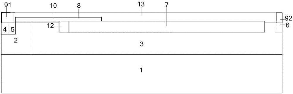
[0038] Such as Figure 4 As shown, the difference between the lateral high-voltage device provided by this embodiment and Embodiment 1 is that the thickness of the high dielectric constant dielectric block 12 described in this embodiment is smaller than the thickness of the shallow trench isolation region, and its upper surface is isolated from the shallow trench The upper surface of zone 7 is in contact. The principle of reducing the hot carrier effect is the same as that of Embodiment 1.


PUM


Abstract

The invention provides a transverse high-pressure device for reducing a hot carrier effect, and belongs to the field of semiconductor power devices. A high dielectric constant medium block is arranged in a shallow channel isolating region of the conventional transverse high-pressure device, so the electric field intensity of a second conduction type of well region close to the high dielectric constant medium block is reduced, the carrier temperature and the impact ionization rate are reduced, the injection of hot carrier into an oxide layer is inhibited, the hot carrier effect of the device is effectively reduced, and the life of the device is prolonged.

Description

technical field [0001] The invention belongs to the field of semiconductor power devices, in particular to a lateral high-voltage device that reduces hot carrier effects. Background technique [0002] Due to its advantages of easy integration and process compatibility, high-voltage power devices have been widely used in industrial control, automotive electronics and other fields. However, when the device works at high drain voltage and gate voltage, a large electric field will be generated in the device channel, so that the carriers in the device channel meet the conditions of becoming hot carriers. When the device works at high voltage Under certain conditions, the large vertical electric field in the device channel will cause the hot carrier effect of the device, resulting in the degradation of the on-resistance, saturation current and other electrical characteristics of the device, shortening the life of the device. The hot-carrier effect is an inevitable problem in high...

Claims


Application Information

Patent Timeline
Patent Type & Authority Applications(China)
IPC IPC(8): H01L29/78H01L29/06
CPCH01L29/78H01L29/0649H01L29/7816
Inventor 乔明周锌祁娇娇张波
Owner UNIV OF ELECTRONICS SCI & TECH OF CHINA
Why Eureka
Try Eureka