Reduced hot carrier induced parasitic sidewall device activation in isolated buried channel devices by conductive buried channel depth optimization

Active Publication Date: 2005-03-15
SAMSUNG ELECTRONICS CO LTD +1
View PDF5 Cites 3 Cited by
  • Summary
  • Abstract
  • Description
  • Claims
  • Application Information

AI Technical Summary

Benefits of technology

A method for reducing hot carrier effects in a transistor device in accordance with the present invention includes the steps of determining a first depth within a junction of the transistor which is sensitive to hot carrier effects, and forming a buried conductive channel at a second depth which is different from the first depth. In other methods, the step of determining the first depth may include the step of analyzing a device structure to determine a position likely to cause hot carrier effects. The step of analyzing may include the steps of performing electrical tests with the second depth at a plurality of different depths, and selecting the depth having best performance. The step of analyzing may include the step of identifying structures likely to cause hot carrier effects. The step of analyzing may include the step of identifying chemical properties likely to cause hot carrier effects

Problems solved by technology

This affects control of the threshold voltage of the gate to be formed, thereby degrading performance of transistor 101 during operation.
However, the proximity of nitride liner 122 to the transistor channel disadvantageously exacerbates the hot carrier reliability problem for P-FET transistors.
As can be appreciated by those skilled in the art, hot carrier reliability problems increase power consumption of the P-FET transistors and, in some cases, may lead to incorrect timing of the circuitry.
For example, the enhanced hot carrier sensitivity is a limiting factor for an aggressive burn-in strategy (for testing manufactured chips) and constrains the device / circuit design.

Method used


Image

  • Reduced hot carrier induced parasitic sidewall device activation in isolated buried channel devices by conductive buried channel depth optimization
  • Reduced hot carrier induced parasitic sidewall device activation in isolated buried channel devices by conductive buried channel depth optimization
  • Reduced hot carrier induced parasitic sidewall device activation in isolated buried channel devices by conductive buried channel depth optimization

Examples


Embodiment Construction

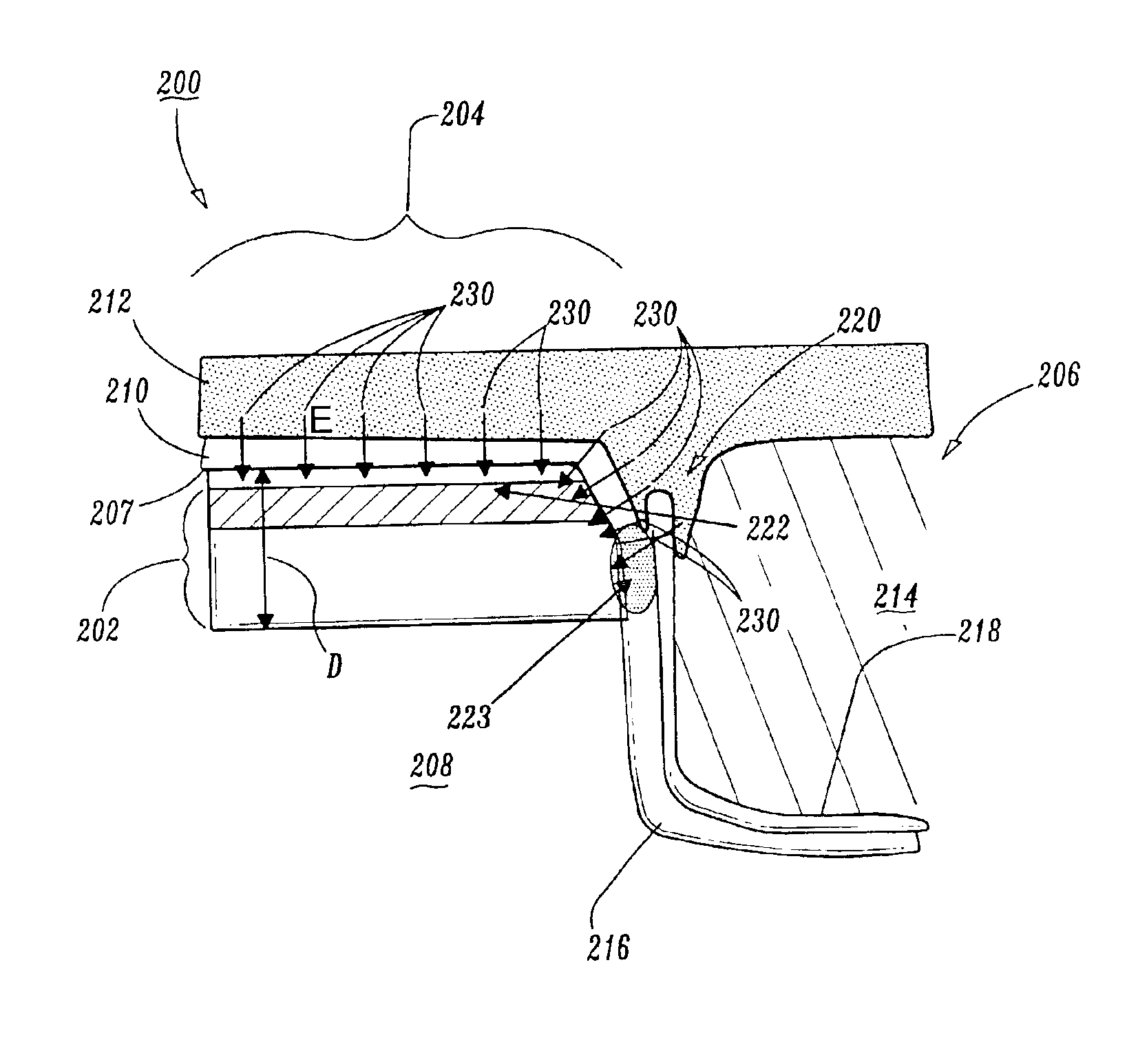
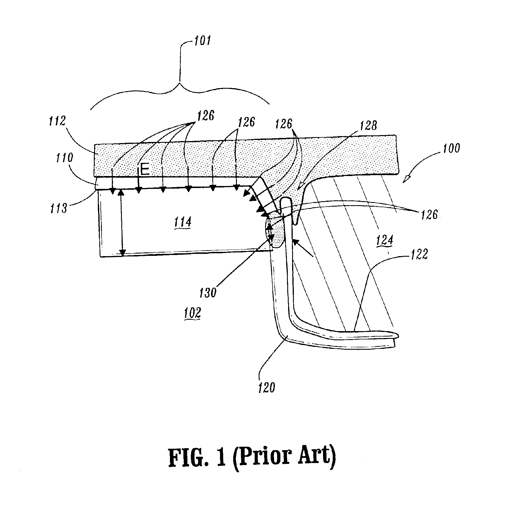
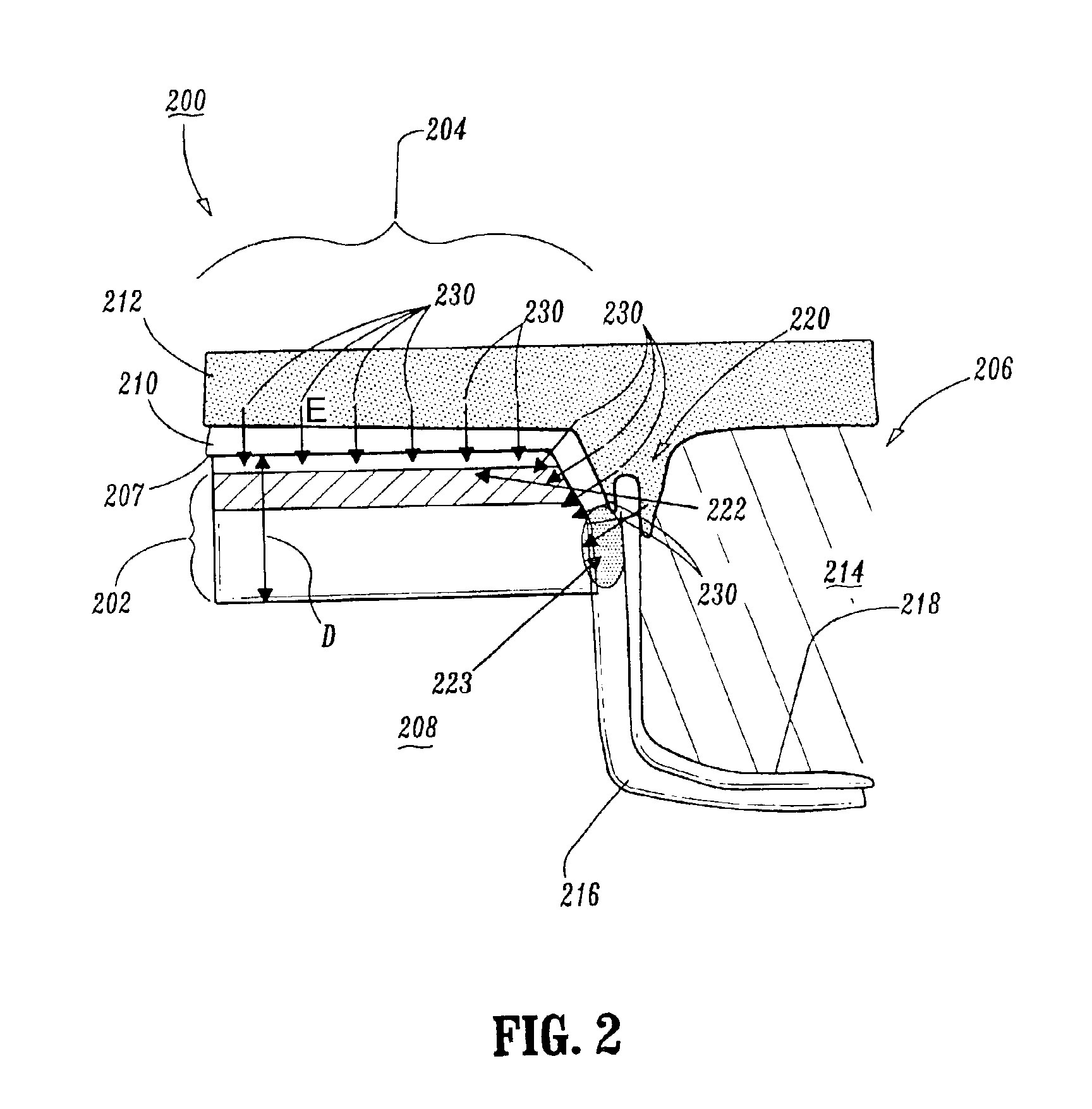
The present invention provides a semiconductor device and structures which reduces or prevents hot carrier reliability problems in a field effect transistor. The present invention advantageously provides a conductive buried channel layer which has its depth adjusted to avoid regions where increased charge trapping may occur. In this way, charge trapping and parasitic junction sidewall leakage are reduced or eliminated. The present invention will be described in terms of a metal oxide semiconductor (MOS) device, in particular a PMOS device, for illustrative purposes, and the present invention should not be construed as being limited to the illustrative examples. It is to be understood that other device types (e.g., NMOS) or device structures may be employed in accordance with the present invention. The present invention may be employed with any semiconductor device, and preferably, in semiconductor devices which employ CMOS technology.

Referring now in specific detail to the drawings ...


PUM


Abstract

A semiconductor device includes a transistor junction formed in a substrate adjacent to an isolation region. A region between the transistor junction and the isolation region includes an area susceptible to hot carrier effects. The transistor junction extends from a surface of the substrate to a first depth. A buried conductive channel layer is formed within the transistor junction between the surface of the substrate and the first depth. The buried conductive channel layer has a peak conduction depth, which is different from a depth of the area susceptible to hot carrier effects.

Description

BACKGROUND1. Technical FieldThis disclosure relates to semiconductor fabrication, and more particularly, to method for reducing hot carrier effects in buried channel metal oxide semiconductor field effect transistor (MOSFET) solid state devices.2. Description of the Related ArtA dynamic random access memories (DRAMs) include an array area which typically has transistors and capacitors. The capacitors are typically configured to store a charge, which can be accessed by appropriate support circuitry associated with the DRAM. Typically, the array circuitry and the support circuitry of the DRAM are located in different areas of the integrated circuit (IC). Although transistors are present in both the array area and the support area of the DRAM, N-FETs (N-channel Field Effect Transistors) are typically employed in the array area, while P-FETs (P-channel Field Effect Transistors) are generally employed in the support circuitry area. The transistors are typically implemented in wells, whic...

Claims


Application Information

Patent Timeline
IPC IPC(8): H01L21/70H01L21/00H01L21/66H01L29/00H01L27/108H01L21/8234H01L27/085H01L27/088H01L21/28H01L21/8242H01L29/78
CPCH01L21/28123H01L29/7838H01L27/10873H10B12/05
Inventor RENEGARAJAN, RAJESHLAROSA, GIUSEPPEDELLOW, MARK
Owner SAMSUNG ELECTRONICS CO LTD
Why Eureka
Try Eureka