Thin film transistor and manufacturing method thereof

A technology for thin film transistors and fabrication methods, which are applied in transistors, semiconductor/solid-state device manufacturing, electrical components, etc., can solve problems such as high cost and complex process, reduce electric field intensity, simplify process process, and suppress hot carrier effect. Effect

Inactive Publication Date: 2019-05-31
WUHAN CHINA STAR OPTOELECTRONICS SEMICON DISPLAY TECH CO LTD
View PDF2 Cites 3 Cited by
  • Summary
  • Abstract
  • Description
  • Claims
  • Application Information

AI Technical Summary

Problems solved by technology

However, this kind of lightly doped drain needs to increase the yellow light process, and two ion implantation procedures are required in the process, the process is more complicated and the cost is higher

Method used


Image

  • Thin film transistor and manufacturing method thereof
  • Thin film transistor and manufacturing method thereof
  • Thin film transistor and manufacturing method thereof

Examples


Embodiment Construction

[0025] The following descriptions of the various embodiments refer to the accompanying drawings to illustrate specific embodiments in which the present disclosure may be practiced. In the figures, structurally similar elements are denoted by the same reference numerals.

[0026] The implementation process of the embodiments of the present disclosure will be described in detail below in conjunction with the accompanying drawings.

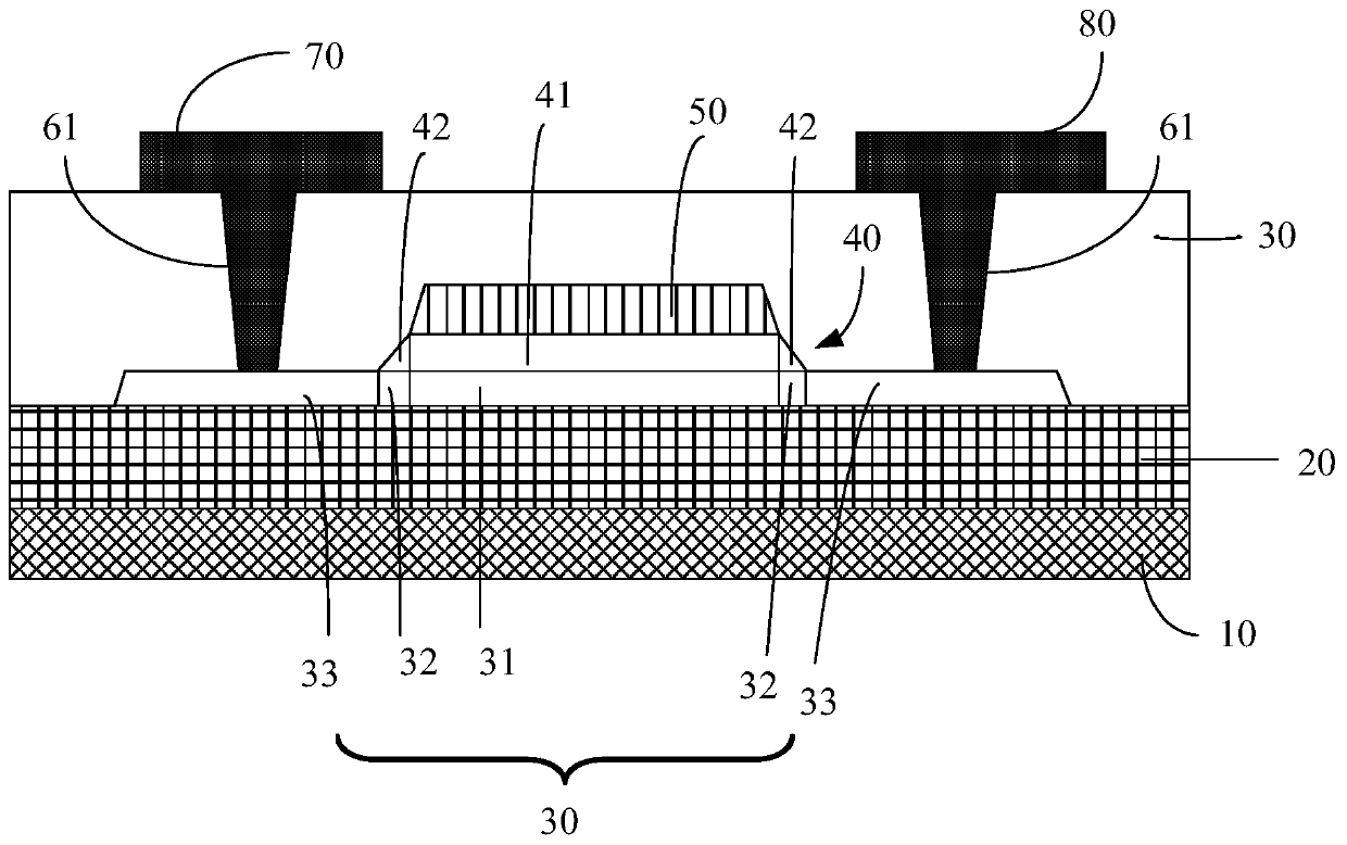
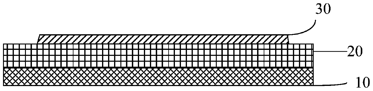
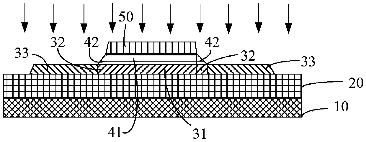
[0027] see Figure 1 to Figure 2A -2C, figure 1 It is a schematic diagram of the structure of the disclosed thin film transistor. Figures 2A-2C It is a schematic flow chart of the manufacturing method of the thin film transistor disclosed herein. The disclosure provides a thin film transistor, comprising: a substrate 10; a buffer layer 20 disposed on the substrate 10; a polysilicon layer 30 disposed on the buffer layer 20, the polysilicon layer 30 comprising a channel region 31, two lightly doped regions 32 arranged on both sides of the channel ...


PUM


Abstract

A thin film transistor comprises a substrate, a buffer layer, a polycrystalline silicon layer, a gate insulating layer, a gate layer, an insulating layer, a source electrode and a drain electrode. Thegate insulating layer comprises a central part and two inclination angle parts arranged in the two sides of the central part respectively, the central part covers a channel region of the polycrystalline silicon layer, the inclination angle portions cover lightly-doped regions of the polycrystalline silicon layer respectively, so that the gate insulating layer forms an inclination angle structurecorresponding to the lightly doped regions. Thus, the thin film transistor is heavily and lightly doped in one doping process. The invention also provides a manufacturing method of the thin film transistor.

Description

technical field [0001] The disclosure relates to the field of display technology, in particular to a thin film transistor and a manufacturing method thereof. Background technique [0002] Low Temperature Poly-silicon (LTPS) thin film transistor (ThinFilm Transistor, TFT) has high carrier mobility and can be used to make small thin film transistor devices. It is the preferred technology for the development of high-resolution small and medium-sized products. [0003] However, with the development trend of higher resolution products and the demand and development of products with higher pixel density, the thin film transistor array substrate is required to have a smaller size, which puts forward higher requirements for the array substrate manufacturing process. Because as the size of the thin film transistor decreases, its electrical characteristics will be unstable or even deteriorated, so that the electrical requirements required by the product cannot be met. For example, wh...

Claims


Application Information

Patent Timeline
Patent Type & Authority Applications(China)
IPC IPC(8): H01L29/786H01L21/336
Inventor 秦芳胡泉
Owner WUHAN CHINA STAR OPTOELECTRONICS SEMICON DISPLAY TECH CO LTD
Why Eureka
Try Eureka