Strain vertical MOS device manufacturing method

A technology of MOS device and manufacturing method, which is applied in semiconductor/solid-state device manufacturing, semiconductor devices, electrical components, etc., can solve problems such as device performance degradation, and achieve the effects of improving gate control capability, increasing transconductance, and improving mobility.

Inactive Publication Date: 2014-06-25
XI AN JIAOTONG UNIV
View PDF6 Cites 4 Cited by
  • Summary
  • Abstract
  • Description
  • Claims
  • Application Information

AI Technical Summary

Problems solved by technology

[0005] The purpose of the present invention is to provide a manufacturing method of a strained vertical MOS device, which solves the problem of device performance degradation due to size reduction, effectively improves carrier mobility, thereby improving device performance

Method used


Image

  • Strain vertical MOS device manufacturing method
  • Strain vertical MOS device manufacturing method
  • Strain vertical MOS device manufacturing method

Examples


Embodiment Construction

[0054] The present invention will be described in detail below in conjunction with the accompanying drawings.

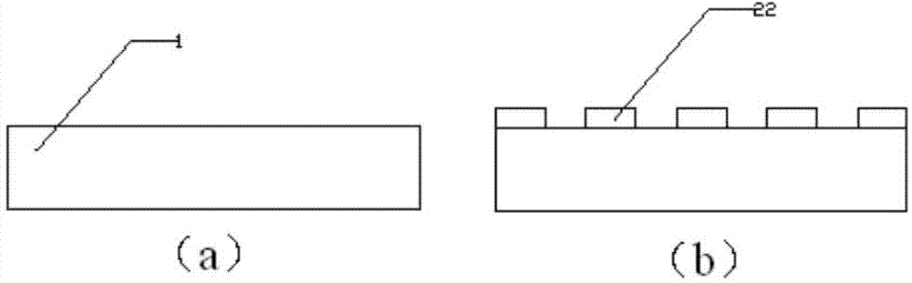
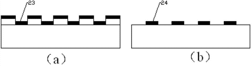
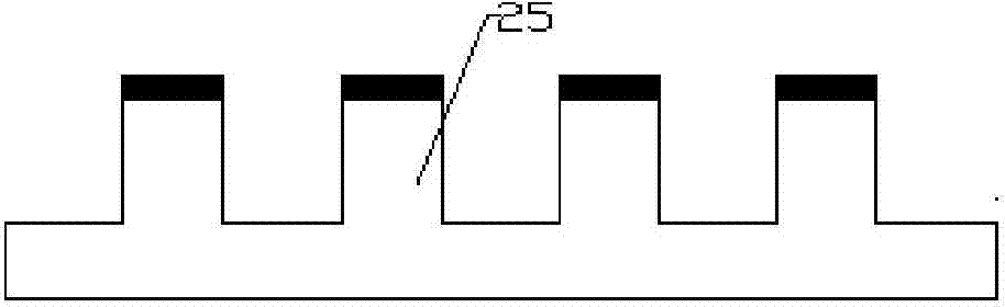
[0055] see Figure 21 and Figure 22 , the strained vertical MOS device manufactured by the present invention includes a substrate 1, a cylindrical channel region vertically arranged on the substrate, a ring-shaped dielectric layer, polysilicon 9, a stress liner layer 5 and a drain conductive layer 3; the drain The conductive layer, the dielectric layer, the gate conductive layer, and the stress liner layer are evenly distributed, and the active conductive layer is arranged on the channel region, and the top of the cylindrical channel region is doped with n+ impurities as the source n+ region 6, doped with n- impurities As the source n-region 7; the drain region is doped with n+ impurities as the drain n+ doped region 2, and doped with n- impurities as the drain n-doped region 10; meanwhile, the cylindrical center of the channel region An asymmetrical Halo-doped so...


PUM

PropertyMeasurementUnit
thicknessaaaaaaaaaa
thicknessaaaaaaaaaa
diameteraaaaaaaaaa

Abstract

Disclosed is a strain vertical MOS device manufacturing method. The method comprises the steps of conducting pattern transfer on a substrate, forming a metal mask, forming a silicon column through etching, reducing the diameter of the silicon column, preparing silicon nanowires and growing a gate oxide layer; conducting polycrystalline silicon deposition, doping and foreign ion activation to form an annular grid electrode; depositing a stress silicon nitride film outside the grid electrode to form a stress liner layer; conducting ion injection to form a drain terminal n- doping area; conducting ion injection on the peripheral annular area of the substrate to form a drain terminal n+ doping area; conducting P+ ion injection on the upper portions of the silicon nanowires to form a Halo doping structure, and conducting n type ion injection to form a source terminal; depositing metal and alloy. According to the method, the grid-control capacity of devices in a nanometer node integrated circuit is improved, the short-channel effect and hot carrier effect are restrained, carrier mobility is improved, current driving capacity is improved, the size of the devices is reduced on the premise that the performance of the devices is not reduced, and then requirements for miniaturization of the devices are met.

Description

technical field [0001] The invention belongs to the field of manufacturing nanometer electronic devices, and relates to a method for forming a strained channel semiconductor device using a stress liner technology, in particular to a method for manufacturing a strained vertical MOS device. Background technique [0002] As the size of semiconductor devices continues to shrink, the method of improving device performance by scaling down the device size is approaching the limit, and the short-channel effect and subthreshold performance degradation also limit the further reduction of the device size. Therefore, many researches are dedicated to new structures and new processes to meet the requirements of chips for device characteristics under the condition of nanometer size. Among all the MOSFET device structures currently proposed, the gate of the surrounding gate MOSFET completely surrounds the channel, which has the strongest short channel effect suppression ability and current ...

Claims


Application Information

Patent Timeline
Patent Type & Authority Applications(China)
IPC IPC(8): H01L21/336H01L29/78B82Y10/00
CPCB82Y40/00H01L29/0676H01L29/66666H01L29/7843
Inventor 李尊朝苗治聪李昕怡张亮亮
Owner XI AN JIAOTONG UNIV
Why Eureka
Try Eureka