MOS transistor and forming method thereof

A technology of MOS transistors and transistors, applied in semiconductor devices, semiconductor/solid-state device manufacturing, electrical components, etc., can solve problems such as increasing the threshold voltage of NMOS transistors, affecting reliability, and degrading semiconductor device performance, so as to reduce substrate leakage current , improve life, reduce the effect of hot carrier effect

Inactive Publication Date: 2015-07-29
SEMICON MFG INT (SHANGHAI) CORP +1
View PDF4 Cites 4 Cited by
  • Summary
  • Abstract
  • Description
  • Claims
  • Application Information

AI Technical Summary

Problems solved by technology

The hot carrier effect will increase the threshold voltage of NMOS transistors, reduce the threshold voltage of PMOS transistors, degrade the performance of semiconductor devices, and affect the reliability of long-term operation
[0004] Therefore, the performance of the existing MOS transistors needs to be further improved

Method used


Image

  • MOS transistor and forming method thereof
  • MOS transistor and forming method thereof
  • MOS transistor and forming method thereof

Examples


Embodiment Construction

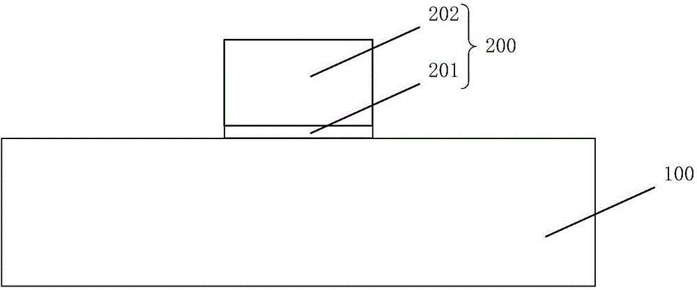
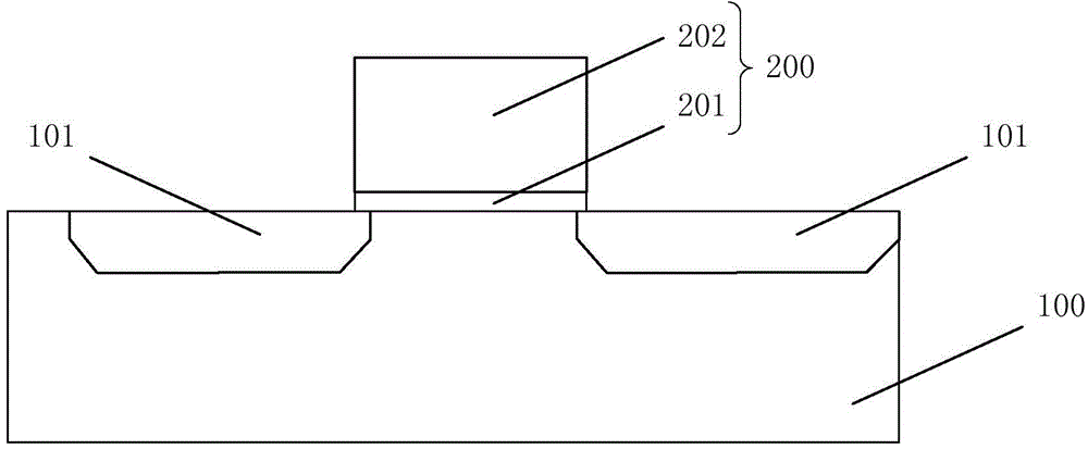
[0028] As mentioned in the background art, the leakage current of the MOS transistor formed in the prior art is relatively high, and the hot carrier effect is significant, so that the performance of the MOS transistor needs to be further improved.

[0029] The short-channel effect of the transistor can be reduced by increasing the channel length to reduce the leakage current of the MOS transistor, but increasing the channel length will increase the channel on-resistance of the MOS transistor, thereby affecting the switching speed of the MOS transistor.

[0030] Research has found that pocket ion implantation can also be carried out in the semiconductor substrate on both sides of the gate structure. The type of doping ions used in the pocket ion implantation is opposite to that of the MOS transistor, and a pocket ion implantation is formed between the source and drain regions and the channel region. The pocket region can suppress the leakage current of the MOS transistor. In or...


PUM


Abstract

Disclosed are a MOS transistor and a forming method thereof. The forming method of the MOS transistor includes the following steps: providing a semiconductor substrate; forming a grid electrode structure on the semiconductor substrate, wherein the grid electrode structure includes a gate dielectric layer on the surface of the semiconductor substrate and a grid electrode on the surface of the gate electric layer, part of the semiconductor substrate, beneath the grid electrode structure, is used as a channel area; carrying out ion implantation in part of the semiconductor substrate, at one side of the grid electrode structure so that a pocket area is formed; forming a source electrode and a drain electrode in parts of semiconductor substrate, at the two sides of the grid electrode structure so that the pocket area is between the source electrode and the channel area, wherein the type of doped ions of the source electrode and the drain electrode is opposite to the type of doped ions in the pocket area. The method is capable of reducing a hot carrier effect of the MOS transistor so that the performance of the transistor is improved.

Description

technical field [0001] The invention relates to the technical field of semiconductors, in particular to a MOS transistor and a forming method thereof. Background technique [0002] Metal-oxide-semiconductor (MOS) transistors are the most basic components in semiconductor manufacturing and are widely used in various integrated circuits. The MOS transistor generally has a symmetrical structure, mainly including: a gate structure located on the surface of the semiconductor substrate, and a source and a drain located in the semiconductor substrate on both sides of the gate structure. The source and drain are formed by high doping, which can be divided into N-type doping (NMOS) and P-type doping (PMOS) according to different device types. [0003] With the development of integrated circuits to ultra-large scale integrated circuits, the circuit density inside integrated circuits is increasing, and the number of components contained is also increasing, and the size of semiconducto...

Claims


Application Information

Patent Timeline
Patent Type & Authority Applications(China)
IPC IPC(8): H01L21/336H01L29/78H01L29/06
CPCH01L29/66477H01L29/0603H01L29/0684H01L29/7833H01L29/7835
Inventor 宋慧芳程勇曹国豪王海强
Owner SEMICON MFG INT (SHANGHAI) CORP
Why Eureka
Try Eureka