Semiconductor device and manufacturing method thereof

A semiconductor and device technology, applied in the field of semiconductor power devices, can solve problems such as limited application and rising on-resistance

Pending Publication Date: 2020-07-03
UNIV OF ELECTRONIC SCI & TECH OF CHINA
View PDF4 Cites 3 Cited by
  • Summary
  • Abstract
  • Description
  • Claims
  • Application Information

AI Technical Summary

Problems solved by technology

However, due to the Ron∝BV2.3~2.6 relationship between the on-resistance Ron of the DMOS device and the device withstand voltage BV, the on-resistance of the device rises sharply when the device is used in high voltage, which limits the lateral high voltage. Application of DMOS devices in high-voltage power integrated circuits, especially in circuits requiring low conduction loss and small chip area

Method used


Image

  • Semiconductor device and manufacturing method thereof
  • Semiconductor device and manufacturing method thereof
  • Semiconductor device and manufacturing method thereof

Examples


Embodiment 1

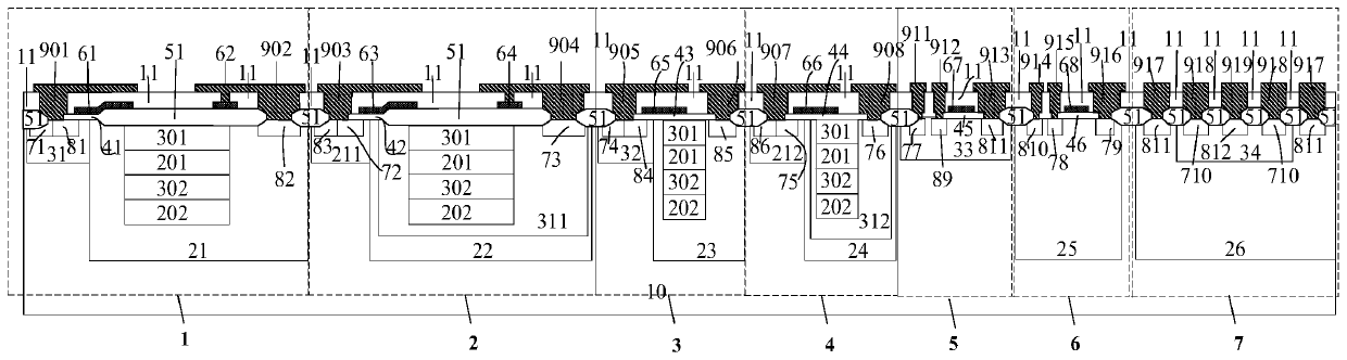
[0047] Such as figure 1As shown, a semiconductor device includes a first-type high-voltage nLDMOS device 1, a first-type high-voltage pLDMOS device 2, a second-type high-voltage nLDMOS device 3, a second-type high-voltage pLDMOS device 4, and a low-voltage NMOS device integrated on the same chip. 5. Low voltage PMOS device 6 and low voltage NPN device 7;

[0048] The first type of high-voltage nLDMOS device 1 is directly made in the p-type substrate 10, and the second n + The contact region 82 is located under the second metal electrode 902 and surrounded by the first n-type deep well 21; under the field oxide layer 51, a first p-type field drop layer 301, a first n-type heavily doped layer 201, a second p-type type drop field layer 302, the second n-type heavily doped layer 202, and the first p-type drop field layer 301, the first n-type heavily doped layer 201, the second p-type drop field layer 302, the second n-type heavily doped layer The doped layers 202 are all surro...

Embodiment 2

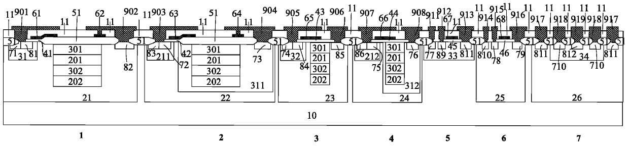
[0073] The difference between this embodiment and Embodiment 1 is: the first n-type well 211 of the device is in the second n-type deep well 22, and the second n-type well 212 is in the fourth n-type well region 24, as figure 2 shown.

Embodiment 3

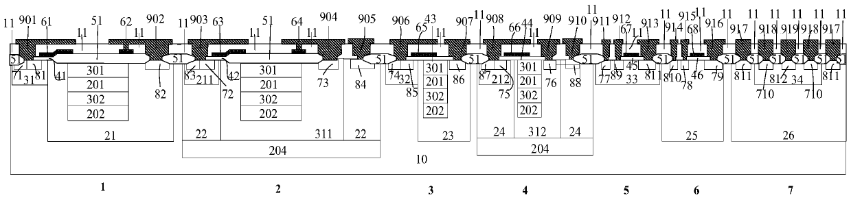
[0075] The difference between this embodiment and Embodiment 2 is that the fourth n+ contact region 84 is surrounded by the second n-type deep well 22, and the first p-type deep well 311 of the device is surrounded by the second n-type well region 22 and the left and right sides of the device. Surrounded by the n-type buried layer 204 at the bottom, the eighth n+ contact region 88 is located in the fourth n-type deep well 24, and the second p-type deep well 312 is surrounded by the fourth n-type well region 24 on the left and right sides and the n-type buried well region at the bottom. Layer 204 surrounds, such as image 3 shown.


PUM

PropertyMeasurementUnit
Thicknessaaaaaaaaaa

Abstract

The invention provides a semiconductor device and a manufacturing method thereof. The semiconductor device comprises a first-class high-voltage nLDMOS device, a first-class high-voltage pLDMOS device,a second-class high-voltage nLDMOS device, a second-class high-voltage pLDMOS device, a low-voltage NMOS device, a low-voltage PMOS device and a low-voltage NPN device which are integrated on the same chip. The first p-type field reduction layer is located on the surface, so that the conductive channel moves downwards, the hot carrier effect is reduced, and the reliability of the device is improved. The n-type heavily doped layer, the p-type field reduction layer, the n-type deep trap, the p-type trap and the p-type substrate form a multiple RESURF structure, the specific on-resistance of thehigh-voltage device is reduced, and the manufacturing cost of the chip is reduced. Compared with a traditional structure without an n-type heavily doped layer, the n-type heavily doped layer has smaller on-resistance under the condition of the same chip area, the on-resistance and the dynamic resistance of the device can be reduced through the n-type heavily doped layer, and the nLDMOS device further has the advantages of being high in input impedance, low in output impedance and the like.

Description

technical field [0001] The invention belongs to the technical field of semiconductor power devices. In particular, a semiconductor device and its manufacturing method. Background technique [0002] The development of high-voltage power integrated circuits is inseparable from high-voltage and low-voltage semiconductor devices. High-voltage power integrated circuits often use the high analog precision of Bipolar transistors, the high integration of CMOS, and the high power or voltage characteristics of DMOS (Double-diffused MOSFET) to integrate Bipolar analog circuits, CMOS logic circuits, CMOS analog circuits and DMOS high-voltage power devices. Monolithically integrated together (referred to as BCD device). Lateral high-voltage devices are widely used in high-voltage power integrated circuits because they are easy to integrate with low-voltage signal circuits through internal connections because the gates and gates are all on the chip surface. However, due to the existenc...

Claims


Application Information

Patent Timeline
IPC IPC(8): H01L29/06H01L27/02
CPCH01L29/063H01L29/0603H01L29/0684H01L27/0203
Inventor 乔明李欣键袁章亦安张波
Owner UNIV OF ELECTRONIC SCI & TECH OF CHINA
Why Eureka
Try Eureka