N-type silicon-on-insulator transverse double-diffusion field effect transistor

A field effect transistor, lateral double diffusion technology, applied in semiconductor devices, electrical components, circuits, etc., can solve the problems of limited buried oxygen layer voltage, easy deviation, increased self-heating effect of devices, etc., to reduce the impact ionization rate and improve reliability. performance, the effect of improving the output characteristic curve

Inactive Publication Date: 2014-04-16
SOUTHEAST UNIV
View PDF3 Cites 0 Cited by
  • Summary
  • Abstract
  • Description
  • Claims
  • Application Information

AI Technical Summary

Problems solved by technology

For SOI LDMOS, the existence of the insulating buried layer brings two problems to the characteristics of the device: one is that the buried oxide layer increases the self-heating effect of the device; Withstand limited voltage
At the same time, the output characteristic curve of high-voltage devices is more likely to deviate from ideal conditions than low-voltage devices

Method used


Image

  • N-type silicon-on-insulator transverse double-diffusion field effect transistor
  • N-type silicon-on-insulator transverse double-diffusion field effect transistor
  • N-type silicon-on-insulator transverse double-diffusion field effect transistor

Examples


Embodiment Construction

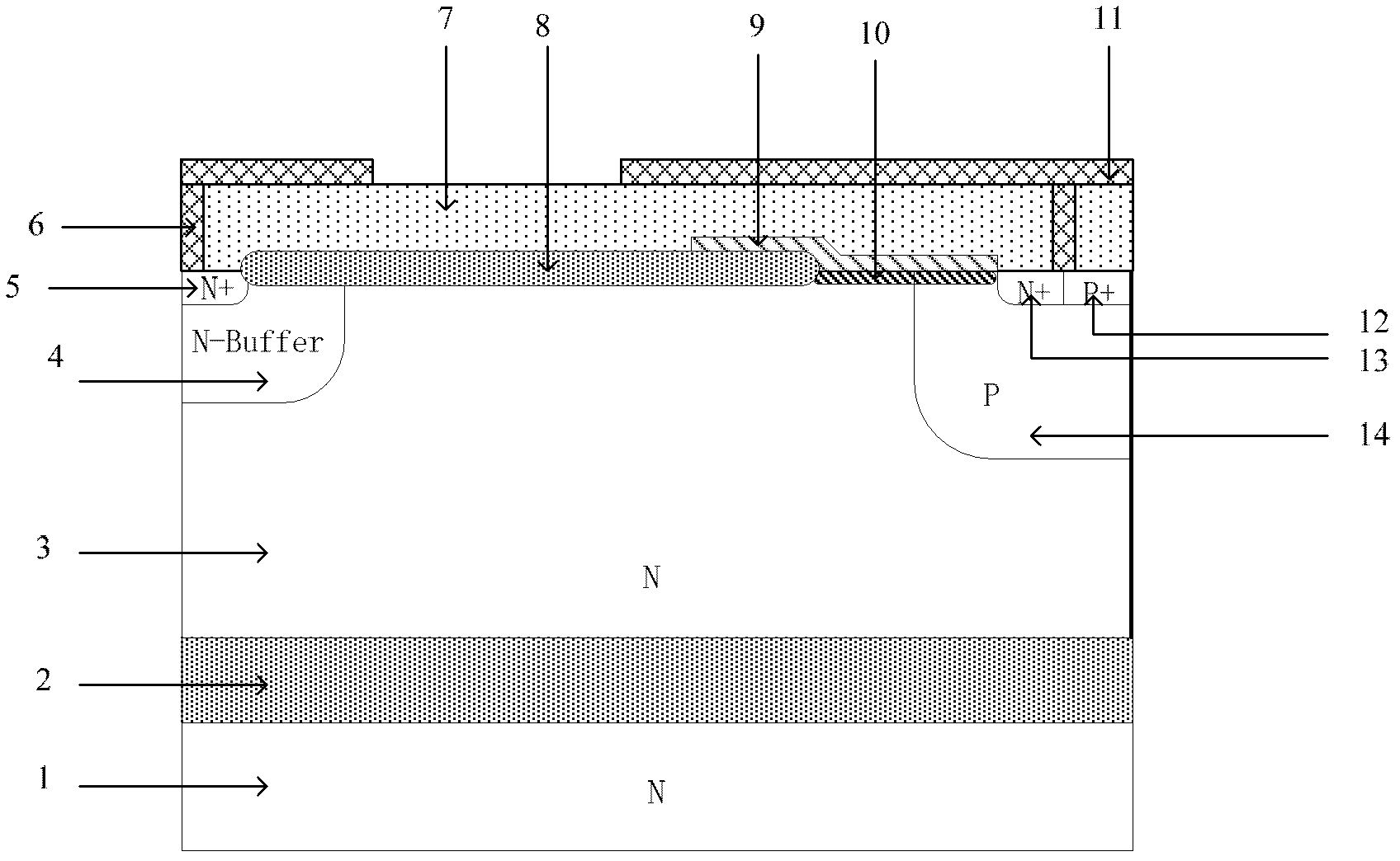
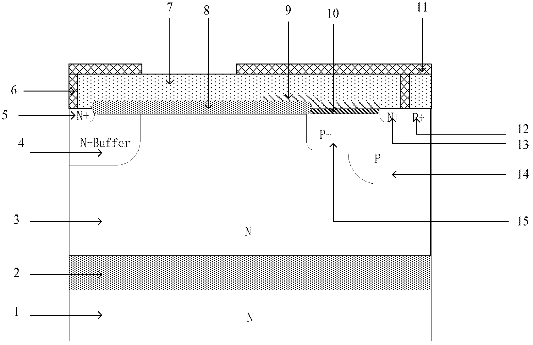
[0021] Attached below figure 2 , the present invention is described in detail, an N-type silicon-on-insulator lateral double-diffused field effect transistor, comprising: an N-type substrate 1, a buried oxygen 2 is arranged on the N-type substrate 1, and a N-type substrate is arranged on the buried oxygen 2. Type epitaxial layer 3 is provided with N-type buffer well 4 and P-type body region 14 in the inside of N-type epitaxial layer 3, is provided with N-type positive region 5 in N-type buffer well 4, is provided with in P-type body region 14 N-type negative region 13 and P-type body contact region 12 are arranged, gate oxide layer 10 and field oxide layer 8 are arranged on the surface of N-type epitaxial layer 3 and one end of gate oxide layer 10 and one end of field oxide layer 8 are offset, so The other end of the gate oxide layer 10 extends toward the N-type cathode region 13 and ends at the N-type cathode region 13, and the other end of the field oxide layer 8 extends tow...


PUM


Abstract

The invention relates to an N-type silicon-on-insulator transverse double-diffusion field effect transistor, which comprises an N underlay, wherein buried oxygen is arranged on the N-type underlay, an N-type extension layer is arranged on the buried oxygen, an N-type buffering well and a P-type body area are arranged inside the N-type extension layer, an N-type anode area is arranged inside the N-type buffering well, an N-type cathode area and a P-type body contact area are arranged inside the P-type body area, a grid oxidized layer and a field oxidized layer are arranged within a given range on the surface of the N-type extension layer, the upper surface of the grid oxidized layer is provided with a polysilicon grid, and a passivation layer and a metal layer are also arranged within a given range on the surface of the transistor. The N-type silicon-on-insulator transverse double-diffusion field effect transistor is characterized in that: the N-type extension layer is also provided with a P-type well area, the P-type well area and the P-type body area form staircase-shaped P-type doping, the doping concentration of the P-type well area is lower than the doping concentration of the P-type body area, one side of the P-type well area is tangential to the field oxidized layer, and the other side of the P-type well area is pushed against the P-type body area. By adopting the structure, the field density and the collision ionization rate at a beak position can be remarkably reduced, so the output characteristics can be effectively improved.

Description

technical field [0001] The invention mainly relates to the field of high-voltage power semiconductor devices, specifically, an N-type silicon-on-insulator lateral double-diffusion field-effect transistor, which is suitable for driving chips in plasma flat panel display equipment, half-bridge driving circuits, and automobile production fields. Background technique [0002] With the continuous improvement of people's living standards, electronic products continue to put forward new requirements for volume, performance, reliability and cost. In this situation, Silicon On Insulator (SOI) process technology came out. Its unique insulating buried layer completely isolates the device from the substrate, reduces the influence of the substrate on the device, and eliminates the latch-up effect of the device. (latch-up) risk, to a large extent alleviates the parasitic effect of silicon devices, greatly improving the performance of devices and circuits. Therefore, the circuit made by S...

Claims


Application Information

Patent Timeline
Patent Type & Authority Patents(China)
IPC IPC(8): H01L29/78H01L29/06
Inventor 孙伟锋刘斯扬王昊叶楚楚陆生礼时龙兴
Owner SOUTHEAST UNIV
Why Eureka
Try Eureka