N type silicon on insulator transverse insulated gate bipolar device

A silicon-on-insulator, bipolar device technology, applied in semiconductor devices, electrical components, circuits, etc., can solve problems such as easy deviation, improve reliability, improve anti-high temperature reverse bias stress, and increase costs.

Inactive Publication Date: 2012-05-02
SOUTHEAST UNIV
View PDF6 Cites 5 Cited by
  • Summary
  • Abstract
  • Description
  • Claims
  • Application Information

AI Technical Summary

Problems solved by technology

At the same time, the output characteristic curve of high-voltage devices is more likely to deviate from ideal conditions than low-voltage devices

Method used


Image

  • N type silicon on insulator transverse insulated gate bipolar device
  • N type silicon on insulator transverse insulated gate bipolar device
  • N type silicon on insulator transverse insulated gate bipolar device

Examples


Embodiment Construction

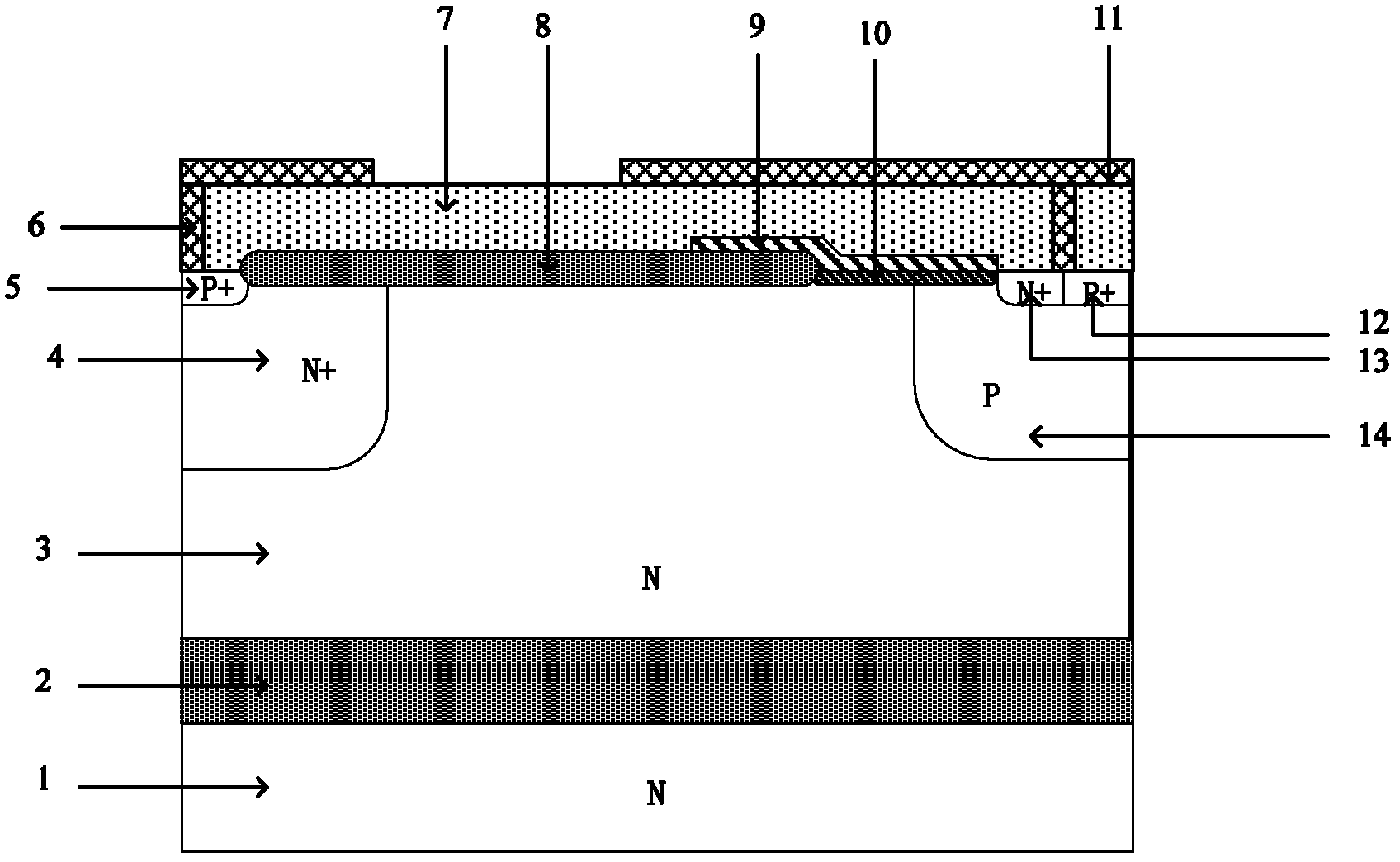
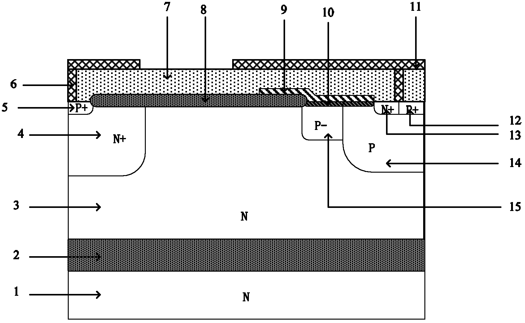
[0021] Attached below figure 2 , the present invention is described in detail, a kind of N-type silicon-on-insulator lateral insulated gate bipolar device, comprising: N-type substrate 1, buried oxygen 2 is arranged on N-type substrate 1, and buried oxygen 2 is provided with The N-type epitaxial layer 3 is provided with an N-type buffer well 4 and a P-type body region 14 inside the N-type epitaxial layer 3, and a P-type anode region 5 is arranged in the N-type buffer well 4, and in the P-type body region 14 An N-type negative region 13 and a P-type body contact region 12 are provided, a gate oxide layer 10 and a field oxide layer 8 are provided on the surface of the N-type epitaxial layer 3, and one end of the gate oxide layer 10 is offset against one end of the field oxide layer 8, The other end of the gate oxide layer 10 extends to the N-type negative region 13 and ends at the N-type negative region 13, and the other end of the field oxide layer 8 extends to the P-type posit...


PUM


Abstract

The invention provides an N type silicon on insulator (SOI) transverse insulated gate bipolar device which comprises an N type substrate. A buried oxide is provided on the N type substrate. An N type epitaxial layer is provided on the buried oxide. The N type epitaxial layer is provided with an N type buffer well and a P type body region inside. The N type buffer well is provided with a P type positive area inside. The P type positive area is provided with an N type positive area and a P type body contact area inside. A surface of the N type epitaxial layer is provided with a gate oxide layer and a field oxide layer in a certain scope. An upper surface of the gate oxide layer is provided with a polysilicon gate. A surface of the device is provided with a passivation layer and a metal level in a certain scope. The device is characterized in that: the N type epitaxial layer is provided with a P type well area, the P type well area and the P type body region form steeped P type doping, dosage concentration of the P type well area is lower than dosage concentration of the P type body area, one side of the P type well area is tangent to the field oxide layer, and the other side of the P type well area presses against the P type body area. According to the above structure, electric field intensity and impact ionization rate of a beak position can be substantially reduced, thus an output characteristic is effectively improved.

Description

technical field [0001] The invention mainly relates to the field of high-voltage power semiconductor devices, specifically, an N-type silicon-on-insulator lateral insulated gate bipolar device, which is suitable for driving chips in plasma flat panel display equipment, half-bridge driving circuits, and automobile production fields. Background technique [0002] With the continuous improvement of people's living standards, electronic products continue to put forward new requirements for volume, performance, reliability and cost. In this situation, Silicon On Insulator (SOI) process technology came out. Its unique insulating buried layer completely isolates the device from the substrate, reduces the influence of the substrate on the device, and eliminates the latch-up effect of the device. (1atch-up) risk, to a large extent alleviates the parasitic effect of silicon devices, greatly improving the performance of devices and circuits. Therefore, the circuit made by SOI process ...

Claims


Application Information

Patent Timeline
Patent Type & Authority Applications(China)
IPC IPC(8): H01L29/739H01L29/06
Inventor 钱钦松刘斯扬万维俊孙伟锋陆生礼时龙兴
Owner SOUTHEAST UNIV
Why Eureka
Try Eureka