A silicon carbide thin film and resistive variable memory

A technology of resistive variable memory and silicon carbide, which is applied in the direction of electrical components, etc., can solve the problems of potential safety hazards, silicon carbide resistive variable memory has not been reported, etc., and achieve the goals of reducing consumption, optimizing resistive characteristics, and increasing defect concentration Effect

Active Publication Date: 2018-10-09
ZHEJIANG NORMAL UNIVERSITY
View PDF3 Cites 0 Cited by
  • Summary
  • Abstract
  • Description
  • Claims
  • Application Information

AI Technical Summary

Problems solved by technology

However, SiH 4 As a highly toxic and explosive gas, although it is an essential raw material for the preparation of silicon-based thin films by CVD, there are great potential safety hazards.
[0004] According to the search, there is no report on the resistive memory based on silicon oxycarbide prepared by magnetron sputtering.

Method used


Image

  • A silicon carbide thin film and resistive variable memory
  • A silicon carbide thin film and resistive variable memory
  • A silicon carbide thin film and resistive variable memory

Examples


Embodiment 1

[0019] Embodiment one: device preparation

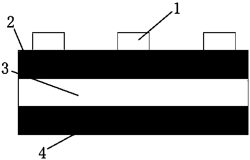
[0020] The schematic diagram of the cross-sectional structure of the resistive memory of the present invention is as follows: figure 1 As shown, the preparation process of the resistive variable memory of this example is described below in conjunction with the schematic cross-sectional structure.

[0021] 1. First, P-type heavily doped silicon wafers with a thickness of 500 μm (resistivity less than ) is cleaned using the RCA standard cleaning method in the IC process.

[0022] 2. Using radio frequency magnetron reactive sputtering 4H-SiC target with a purity of 99.5%, a resistive dielectric layer SiC with a thickness of about 20nm was prepared at room temperature x o y , where x=1.21, y=1.45. Parameters: background vacuum -4 , working pressure=0.5Pa, argon flow=30sccm, RF frequency=13.56MHz, RF power=100W, growth time=10min.

[0023] 3. Define the shape and size of the top electrode (a circle with a diameter of 1 mm) using a m...

Embodiment 2

[0026] Embodiment 2: Device detection

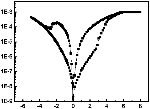
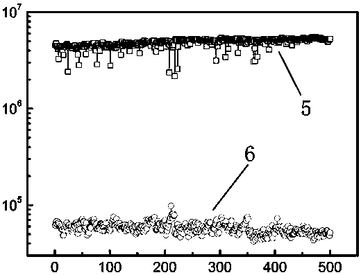
[0027] This embodiment tests the resistive switching characteristics of the resistive memory made in Example 1, and the test results are as follows figure 2 , image 3 with Figure 4 as shown, image 3 Among them, the abscissa represents the number of erasing and writing, the ordinate represents the resistance, the unit is ohm, 5 represents the high-resistance state curve, and 6 represents the low-resistance state curve; Figure 4 , the abscissa represents the retention time, in seconds, the ordinate represents the resistance, in ohms, 5 represents the high-resistance state curve, and 6 represents the low-resistance state curve.

[0028] Depend on figure 2 It can be seen that with the cycle of DC scanning voltage, the device Ag / SiC 1.21 o 1.45 / p + -The resistance of Si will change from high resistance state to low resistance state, reflecting the storage of data 0 and 1.

[0029] Depend on image 3 with Figure 4 It can be s...

Embodiment 3

[0030] Embodiment three: device preparation

[0031] This example uses the same method as Example 1 to prepare a resistive variable memory, and the prepared device has the same structure as Example 1, the difference is that the flow rate of argon gas is 29.9 sccm, and the flow rate of oxygen gas is 0.1 sccm, so that the resistance of this example is Variable dielectric layer SiC x o y x:y=0.72:1.76. The resistive switching characteristic test described in the second embodiment is carried out on the prepared device, and it is found that the device can well meet the requirement.


PUM

PropertyMeasurementUnit
thicknessaaaaaaaaaa
thicknessaaaaaaaaaa
thicknessaaaaaaaaaa

Abstract

The invention provides a resistive variable material and a resistive variable memory based on a silicon oxycarbide thin film. A silicon oxycarbide thin film resistive material, its molecular formula is SiCxOy, where x=1.21~0.21, y=1.45~2.01, and x and y are negatively correlated; the film thickness is below 50nm. A resistive variable memory, comprising a top electrode, a resistive medium layer, a substrate and a back electrode, characterized in that the resistive medium layer is the aforementioned silicon oxycarbide film. Materials such as Ag and Al can be used for the top electrode. In the present invention, materials compatible with the COMS process are selected to prepare the resistive variable memory. The preparation process mainly adopts physical deposition thin film equipment without high-temperature process, thereby reducing energy consumption. By controlling the gas ratio, silicon oxycarbide films with different defect concentrations can be obtained. For the SiC0.21O2.01 material, its on-off ratio reaches 500, which can fully meet the actual needs (greater than 10). At the same time, the resistive memory based on the silicon oxycarbide material has a self-rectification effect, which is helpful for simplifying the design of the external circuit. Significance.

Description

technical field [0001] The invention belongs to the technical field of ultra-large-scale integrated circuits, and in particular relates to a silicon oxycarbide thin film with stable resistive switching characteristics, and a resistive variable memory using the thin film. Background technique [0002] As people continue to put forward requirements on the storage capacity, speed, power consumption, reliability and other performance of non-volatile memory, the FLASH memory based on the traditional floating gate structure is facing a huge challenge because the size cannot be further reduced. A typical resistive memory has a simple "sandwich structure" - a resistive layer is sandwiched between two layers of metal electrodes. As the applied voltage changes, the resistive memory can switch between a high-resistance state and a low-resistance state. , and then achieve the purpose of data 0 and 1 storage. Due to the characteristics of simple structure, high storage density, fast rea...

Claims


Application Information

Patent Timeline
Patent Type & Authority Patents(China)
IPC IPC(8): H01L45/00
CPCH10N70/883H10N70/026
Inventor 黄仕华陈达
Owner ZHEJIANG NORMAL UNIVERSITY
Why Eureka
Try Eureka