Recovery method for image distortion resulting from column delay of image sensor

An image sensor and image distortion technology, applied in image communication, TV, color TV components and other directions, can solve the problems of unrealizable clock wiring, affecting surrounding circuits, consumption, etc., to achieve good recovery and calibration effect, realize acquisition function, The effect of expanding the scope of application

Active Publication Date: 2016-10-12
TIANJIN UNIV
View PDF3 Cites 3 Cited by
  • Summary
  • Abstract
  • Description
  • Claims
  • Application Information

AI Technical Summary

Problems solved by technology

For a long line array image sensor, the same number of clock tree paths as the number of pixels is required, which will consume more chip area. For a Time Delay Integration (TDI) image sensor using line array technology, each pixel The gap between them is so narrow that this clock routing is not achievable
And there will be a large coupling capacitance between the metal lines, which will affect the surrounding circuits

Method used


Image

  • Recovery method for image distortion resulting from column delay of image sensor
  • Recovery method for image distortion resulting from column delay of image sensor
  • Recovery method for image distortion resulting from column delay of image sensor

Examples


Embodiment Construction

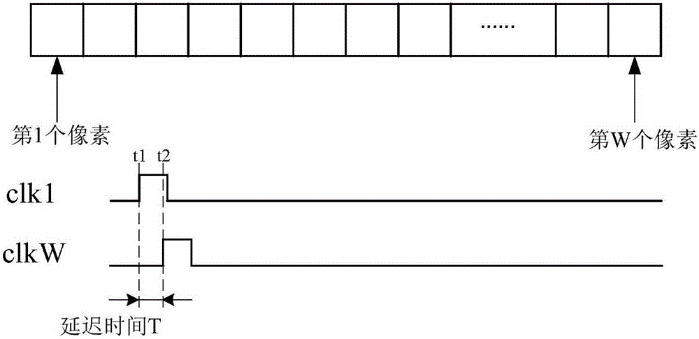
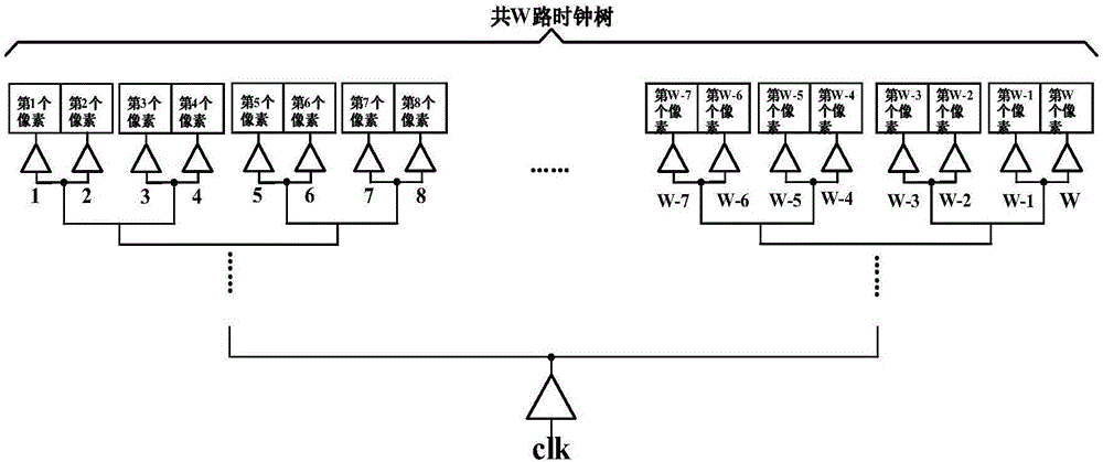
[0022] In the present invention, inspired by the existing Time to Digital Converter (TDC) technology, using the traditional clock signal loading method, by calculating the ratio of the maximum distortion distance of the image edge to the length of the image sensor array, a A method for recovering distorted images.

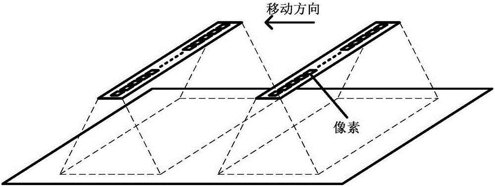
[0023] For the convenience of subsequent analysis, the definitions of some commonly used parameters in the line array image sensor will be given below. The pixel array of the linear image sensor is a one-dimensional linear array structure, such as Figure 4 As shown, the relative moving direction between the pixel array and the scanned object is called Along-Track-Direction, and the direction perpendicular to the relative moving direction is called Across-Track-Direction. In a CMOS image sensor, the shape of a pixel is generally a square, and the pixel center distance is p. Assuming that the light emitted or reflected by the object to be photographed is focused on...


PUM


Abstract

The invention relates to the design field of an analog integrated circuit. In order to enable a linear array type image sensor to realize a high-speed and high-definition image collection function well, improve the line frequency of the linear array type image sensor and expand the application of the linear array type image sensor, the technical scheme provided by the invention is that a recovery method for image distortion resulting from column delay of the image sensor comprises the steps of 1), calculating a maximum distortion distance L along an across-track-direction; 2), calculating a deformation distortion angle alpha of a photographed image, wherein the deformation distortion angle alpha is calculated through the linear array length W of the image sensor and the maximum distortion distance L along the across-track-direction, and the deformation distortion angle alpha is expressed by a formula described in the abstract; and 3), recovering the photographed image according to the deformation distortion angle alpha. The method is mainly applied to image processing.

Description

technical field [0001] The invention relates to the field of analog integrated circuit design, in particular to the design of an imaging calibration circuit for a high-speed long line array image sensor. Specifically, it relates to a recovery method for image distortion caused by image sensor column delay. Background technique [0002] The image sensor can convert the optical signal obtained by the lens into an electrical signal that is easy to store, transmit and process. According to the pixel arrangement structure in the solid-state image sensor chip, the image sensor can be divided into an area array image sensor and a line array image sensor. [0003] The area array image sensor directly captures the object through the pixels arranged in the form of a two-dimensional area array to obtain two-dimensional image information. Each exposure of the area array image sensor can obtain a complete frame of image, which can easily obtain two-dimensional image information, but th...

Claims


Application Information

Patent Timeline
IPC IPC(8): H04N5/232H04N5/353
CPCH04N23/684H04N25/53
Inventor 徐江涛史晓琳聂凯明高静高志远史再峰
Owner TIANJIN UNIV
Why Eureka
Try Eureka