
Circuit arrangement and method for controlling a junction field effect transistor

A field effect transistor and circuit arrangement technology, applied in the direction of using electrical devices, thermometers using electrical/magnetic components directly sensitive to heat, using electromagnetic means, etc., can solve problems such as being unsuitable for actual operation, and achieve the effect of avoiding interruptions

Active Publication Date: 2020-01-21
VALEO EAUTOMOTIVE GERMANY GMBH
View PDF6 Cites 0 Cited by
  • Summary
  • Abstract
  • Description
  • Claims
  • Application Information

AI Technical Summary

Problems solved by technology

However, this mode of operation is not suitable for practical operation because the body diode carries freewheeling current or reverse current during operation

Method used


Image

  • Circuit arrangement and method for controlling a junction field effect transistor
  • Circuit arrangement and method for controlling a junction field effect transistor
  • Circuit arrangement and method for controlling a junction field effect transistor

Examples


Embodiment Construction

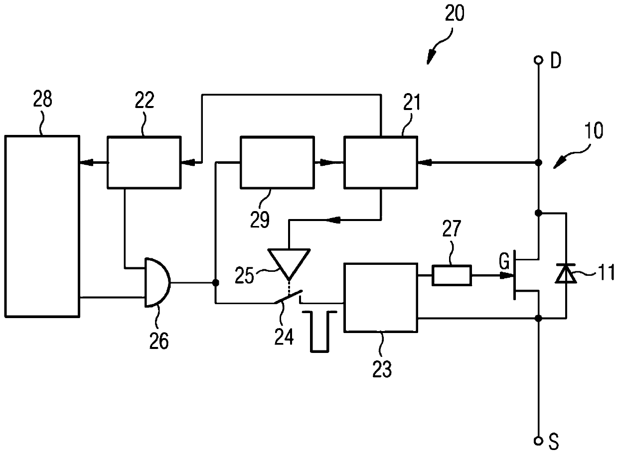
[0024] figure 1 An exemplary embodiment of a circuit arrangement 20 according to the invention for controlling a junction field effect transistor 10 is shown. The junction field effect transistor 10 may be, for example, a silicon carbide field effect transistor (SiC-JFET). The JFET 10 comprises a control connection G (gate) and a first main connection D (drain) and a second main connection S (source). A channel is formed between the first main terminal D and the second main terminal S, and when the JFET 10 is switched on, current can flow through the channel. The body diode present between the second main connection (S) and the first main connection (D) is indicated with 11 .

[0025] The control connection G, for example a junction field effect transistor, is connected to a p-conduction region arranged in an n-conduction (substrate) material. The p-type conduction region and the n-type conduction material of the JFET form a p-n diode. A Junction Field Effect Transistor (J...


PUM


Abstract

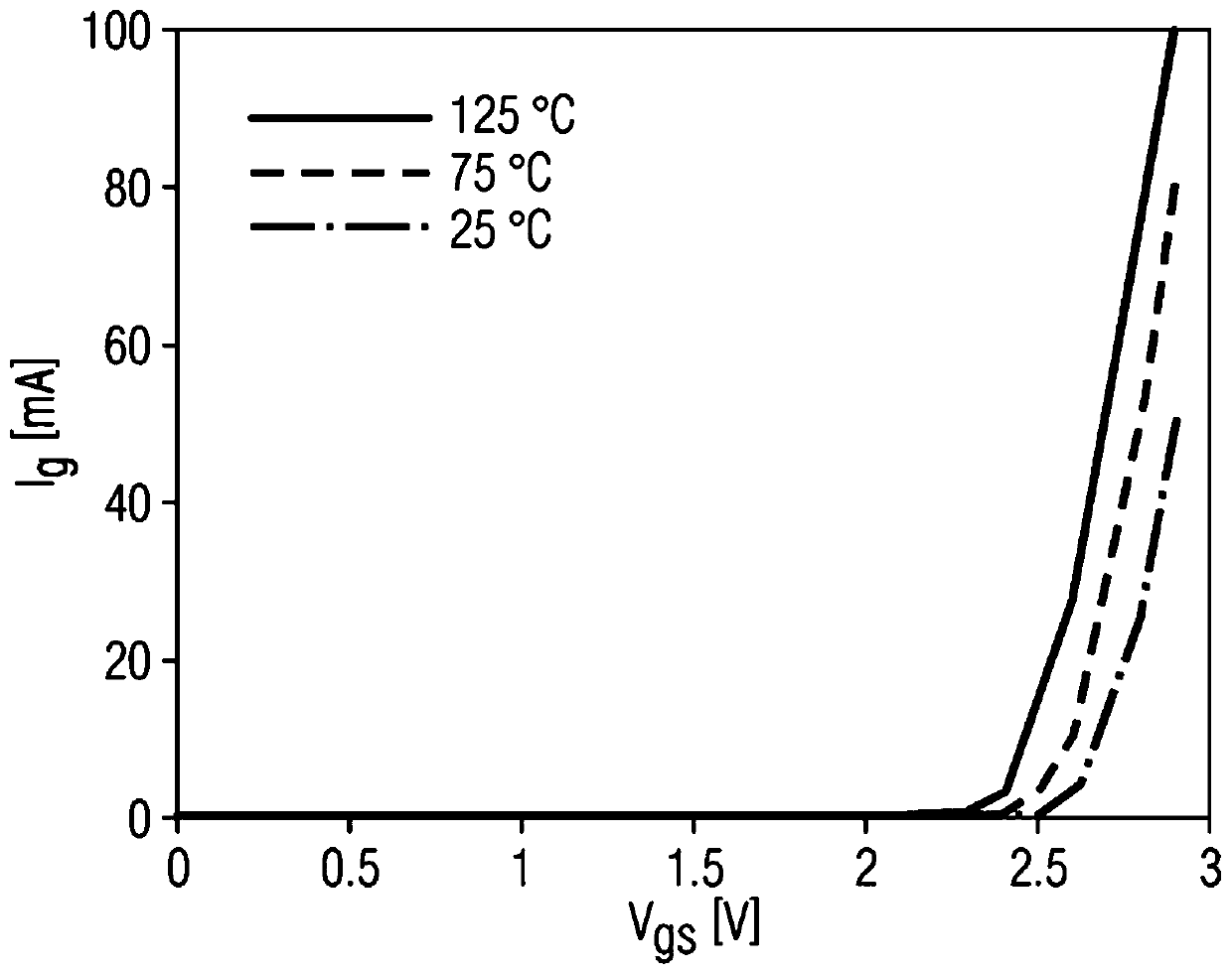
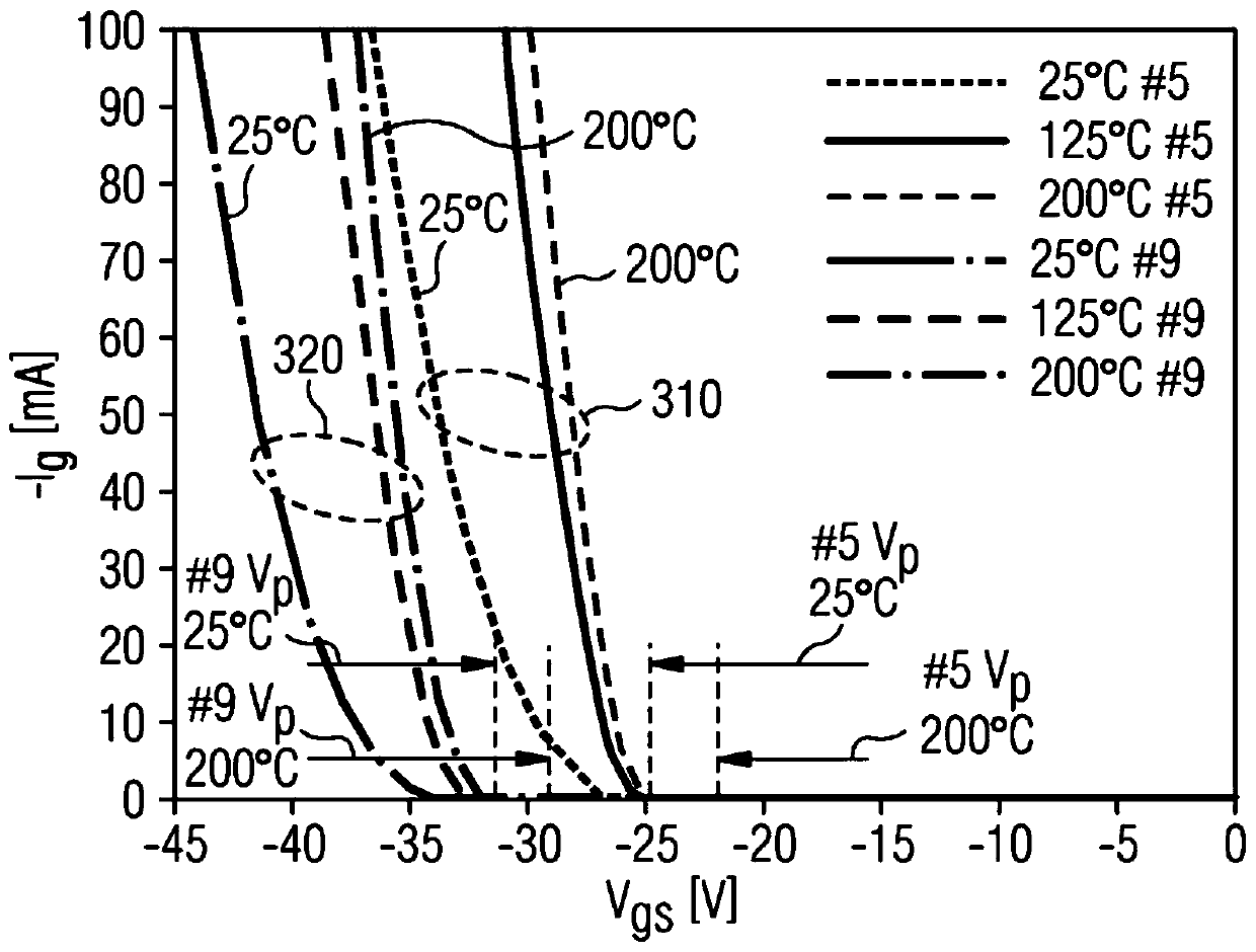
The invention describes a circuit arrangement for controlling a junction field effect transistor (10) comprising a control terminal (G) and a first main terminal (D) and a second main terminal (S), in which A channel is formed between them. The circuit arrangement includes: a unit (21, 22, 24, 25, 26, 27, 28) for generating a control signal by means of which the junction field effect transistor (10) is placed in a first switching state (conducting) and the second switching state (off) alternately switching back and forth. The circuit arrangement includes a unit (23) for current evaluation, which is connected between a control connection (G) and a second main connection (S). The unit (23) for current evaluation is designed as a unit (21) for generating a control signal when or as soon as there is a transition from a first switching state (on) to a second switching state (off). ,22,24,25,26,27,28) The voltage (V) applied between the control terminal (G) and the second main terminal (S) gs ) is controlled to exceed the punch-through voltage, measure the reverse current (I) flowing through the control connector (G) g ), and according to the measured current (I g ) determines the absolute temperature of the junction field effect transistor (10).

Description

technical field [0001] The invention relates to a circuit arrangement and a method for controlling a semiconductor switching element in the form of a junction field effect transistor comprising a first main connection and a second main connection and forming a channel therebetween. Background technique [0002] Semiconductor switching elements are used, for example, as power switching elements. Therein lies the need to monitor the temperature of the semiconductor switching element so that the semiconductor switching element and the module comprising the semiconductor switching element (also referred to as a system) as a whole can function reliably. In the event of excessive temperatures, the circuit arrangement controlling the semiconductor switching elements must ensure reliable switching off. [0003] For this purpose, for example, an external temperature sensor such as an NTC temperature sensor is used. It is arranged, for example, on a carrier plate in a module contain...

Claims


Application Information

Patent Timeline
Patent Type & Authority Patents(China)
IPC IPC(8): H03K17/08G01K7/01
CPCG01K7/01H03K17/08H03K2017/0806H03K2017/6875
Inventor A.梅尔康扬
Owner VALEO EAUTOMOTIVE GERMANY GMBH
Learn More