Surface shape detection device and detection method

A technology of surface shape detection and area measurement, which is applied in the direction of measuring devices, optical devices, instruments, etc., can solve the problems of inability to measure strongly curved surfaces, low measurement accuracy, and low measurement range

Active Publication Date: 2016-10-26
INST OF HIGH ENERGY PHYSICS CHINESE ACADEMY OF SCI
View PDF5 Cites 8 Cited by
  • Summary
  • Abstract
  • Description
  • Claims
  • Application Information

AI Technical Summary

Problems solved by technology

For any kind of surface shape measurement equipment, limited by the limited number of pixel arrays of the detection sensing element, there is a contradiction between measurement accuracy and measurement range, that is, a device with high measurement accuracy has a low measurement range, while a device with a high measurement range, Its measurement accuracy is low
[0003] At the same time, existing synchrotron radiation optical element surface shape detection methods, such as interferometers, cannot measure strongly curved surfaces (large deformation range), and long-range surface shape instruments based on thin beam scanning can only provide surface shape on a one-dimensional scale. Variety

Method used


Image

  • Surface shape detection device and detection method
  • Surface shape detection device and detection method
  • Surface shape detection device and detection method

Examples


Embodiment Construction

[0037] The application will be further described in detail below in conjunction with the accompanying drawings and embodiments. It should be understood that the specific embodiments described here are only used to explain related inventions, rather than to limit the invention. It should also be noted that, for ease of description, only parts related to the invention are shown in the drawings.

[0038] It should be noted that, in the case of no conflict, the embodiments in the present application and the features in the embodiments can be combined with each other. The present application will be described in detail below with reference to the accompanying drawings and embodiments.

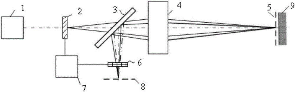
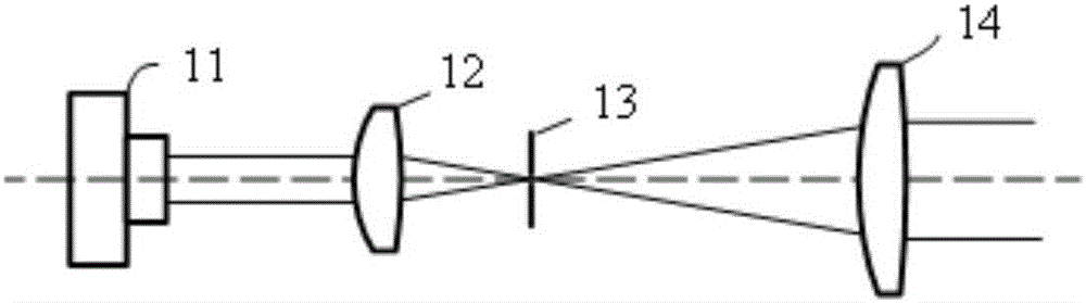
[0039] refer to Figure 1 to Figure 3 , the invention provides a surface shape detection device, comprising:

[0040] Laser light source assembly 1, which provides collimated laser light;

[0041] a wavefront encoder 2, which is used to modulate the laser light provided by the laser light source...


PUM


Abstract

The invention discloses a surface shape detection device and a detection method. The surface shape detection device comprises a laser light source assembly, a wavefront encoder, a light splitter, a lens, an array detector and a control module. The surface shape detection method comprises the following steps: light emitted by the laser light source assembly irradiates the wavefront encoder; the emergent light obtained after modulation of the wavefront encoder passes through the light splitter and the lens and is imaged to one surface of a region to be detected; the light reflected by the surface passes through the lens and the light splitter and enters the array detector; the control module controls the wavefront encoder to generate sequentially-moving light spots on the surface of the region to be detected; the array detector records and keeps the image of the light spot of each sampling point, and converts the received light into electrical signals; and the control module carries out corresponding processing on the electrical signals and obtains inclination angle of the surface of an object to be detected. The method and system can realize switching between a high-precision small-range mode and a low-precision large-range mode, can measure two-dimensional bodies and are suitable for online detecting optical elements arranged on a synchrotron radiation beam line.

Description

technical field [0001] The present disclosure relates to the field of two-dimensional surface shape detection of mirror objects, in particular to a surface shape detection device and detection method. Background technique [0002] In the field of synchrotron radiation, a large number of optical elements, such as mirrors and monochromators, are used on the beamline for propagating and modulating X-ray beams. Surface shape errors of optical components, especially inclination errors, affect beam quality. In order to improve the performance of the synchrotron radiation device, the beamline must be adjusted on the basis of the surface shape measurement. For any kind of surface shape measurement equipment, limited by the limited number of pixel arrays of the detection sensing element, there is a contradiction between measurement accuracy and measurement range, that is, a device with high measurement accuracy has a low measurement range, while a device with a high measurement rang...

Claims


Application Information

Patent Timeline
Patent Type & Authority Applications(China)
IPC IPC(8): G01B11/24
CPCG01B11/24
Inventor 杨福桂李明盛伟繁刘鹏
Owner INST OF HIGH ENERGY PHYSICS CHINESE ACADEMY OF SCI
Why Eureka
Try Eureka