Method for separating substrate and bearing panel of electronic device and bearing panel
An electronic device and panel technology, applied in the display field, can solve problems such as the deviation of two substrates and the damage of the display panel, and achieve the effects of not being easy to align deviation, non-destructive separation, and not easy to deform
- Summary
- Abstract
- Description
- Claims
- Application Information
AI Technical Summary
Problems solved by technology
Method used
Image
Examples
no. 1 example
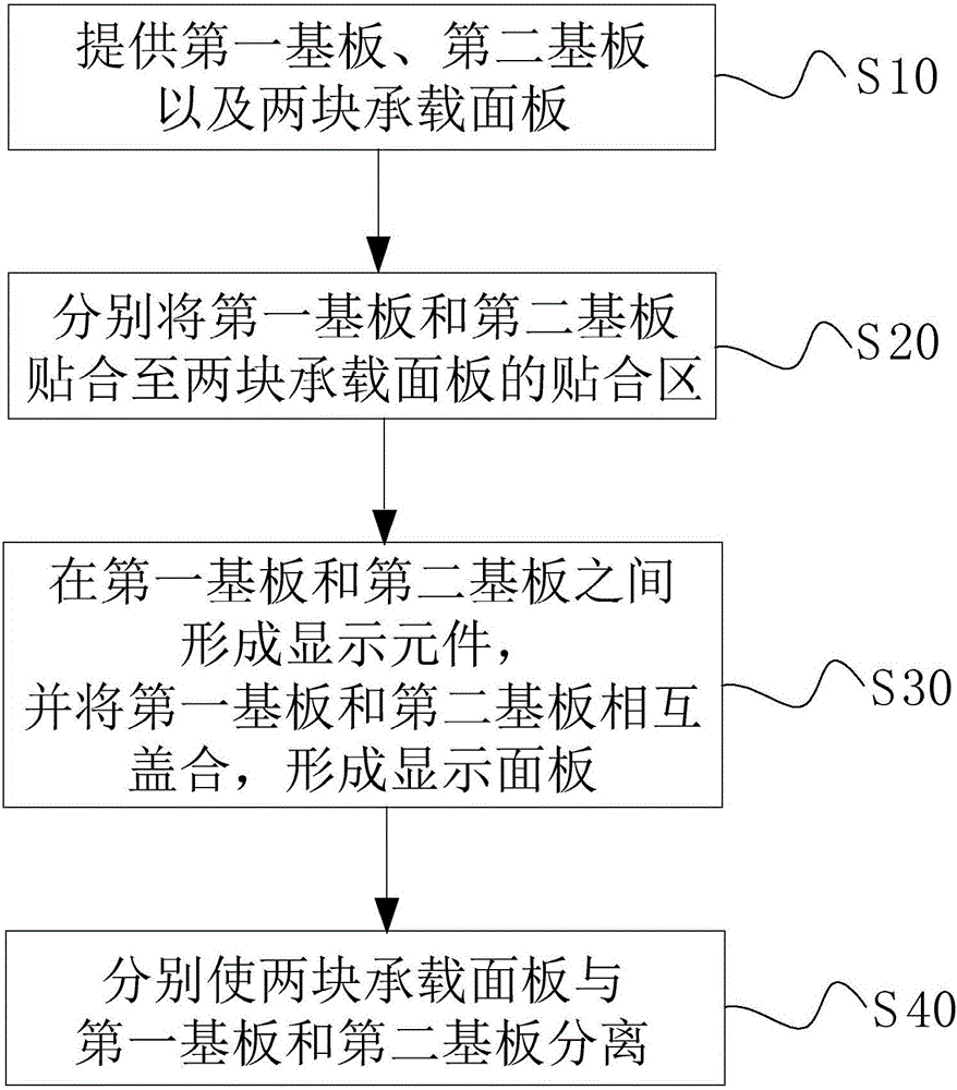
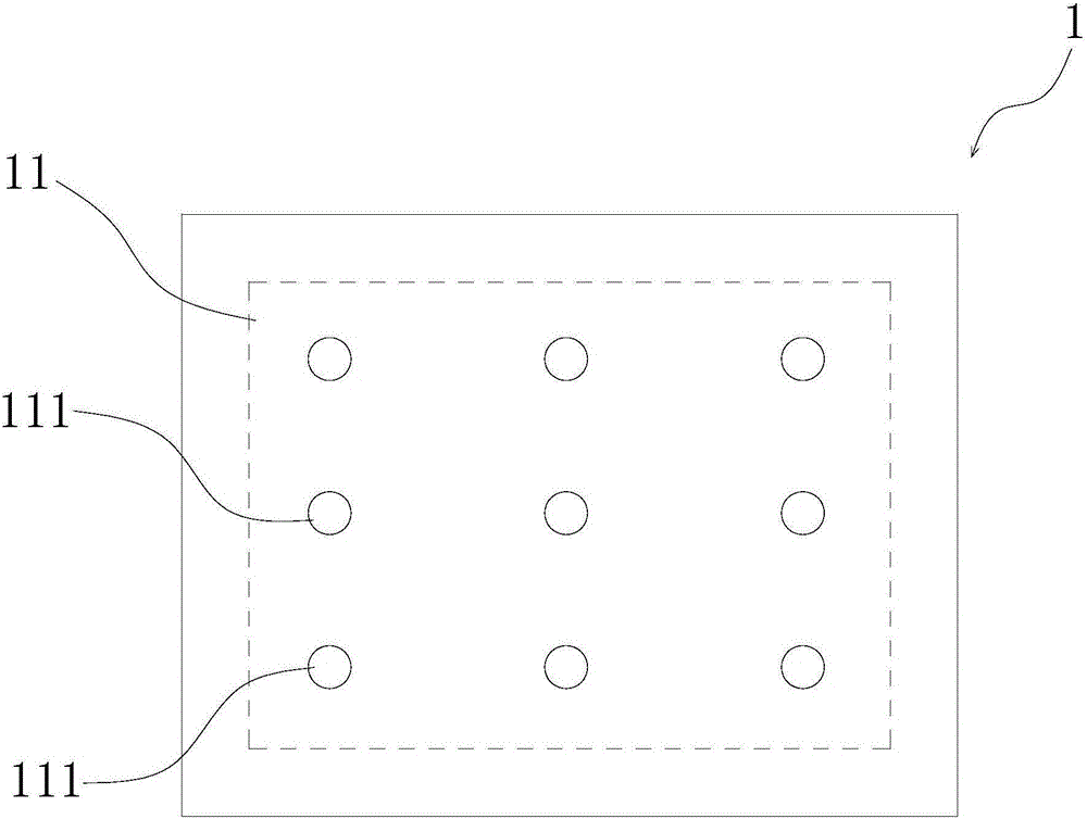
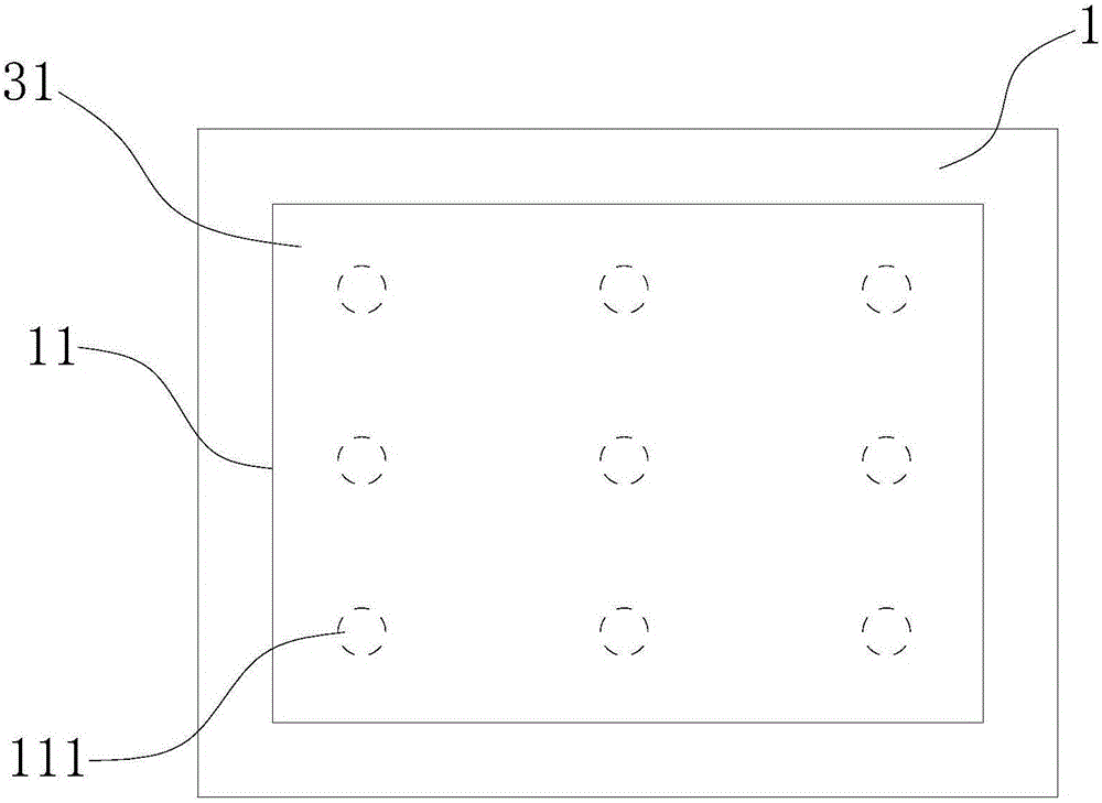
[0029] See figure 1 to Figure 4, figure 1 A flow chart showing a method for manufacturing a display panel in a first embodiment of the present invention, figure 2 A schematic structural view of the bearing panel in the first embodiment of the present invention is shown. image 3 A schematic structural view of the lamination of the carrying panel and the first substrate in the first embodiment of the present invention is shown. Figure 4a with Figure 4b A schematic cross-sectional structure diagram and a top view of the display panel formed after the first substrate and the second substrate are covered in the first embodiment of the present invention are respectively shown. Such as figure 1 As shown, in an embodiment of the present invention, the manufacturing method of the display panel includes the following steps:
[0030] Step S10: providing a first substrate, a second substrate and two carrying panels. Specifically, as figure 2 As shown, the carrying panel 1 prov...
no. 2 example
[0042] The second embodiment of the present invention is another embodiment of the method for separating the substrate of the display panel and the carrying panel of the present invention, which is the same as the above-mentioned Figure 5 with Image 6 What is different from the first embodiment shown is that in this embodiment, the carrying panel is separated from the first substrate by applying pressure to the through hole of the carrying panel by using a thimble.
[0043] Please also see Figure 7 with Figure 8 , which respectively show the flow chart of the method for separating the substrate of the display panel and the carrying panel and the structure diagram after inserting the thimble into the through hole of the carrying panel according to the second embodiment of the present invention. Similarly, Figure 8 The method for separating the substrate of the display panel and the carrying panel of the present invention is also described by taking the separation of the...
no. 3 example
[0050] The third embodiment of the present invention is another embodiment of the method for separating the substrate of the display panel from the carrying panel of the present invention, which is the same as the above-mentioned Figure 5 with Image 6 The difference of the first embodiment shown is that in this embodiment, the connection between the bearing panel and the first substrate is achieved by fixing the bearing panel to the opening of a sealed box and increasing the pressure in the sealed box, and the pressure passes through the through hole Transfer to the first substrate to realize the separation between the carrying panel and the first substrate.
[0051] Please also see Figure 9 with Figure 10 , which respectively show the flow chart of the method for separating the substrate of the display panel and the carrying panel and the structural diagram after fixing the carrying panel to the sealing box according to the third embodiment of the present invention. Si...
PUM
 Abstract
Description
Claims
Application Information


