
Method of dividing wafer

A technology for wafers and dicing lanes, which is applied in the field of wafer division, can solve the problems of increased cost and complicated wafer processing procedures, and achieves the effect of reducing costs

Inactive Publication Date: 2016-10-26
DISCO CORP
View PDF9 Cites 11 Cited by
  • Summary
  • Abstract
  • Description
  • Claims
  • Application Information

AI Technical Summary

Problems solved by technology

[0010] However, when performing the resist film forming step and the resist film removing step separately, as described above, it is necessary to use different devices such as a resist film forming device and a polishing device, so the processing steps of the wafer are divided into two parts. is complicated, and the cost also increases

Method used


Image

  • Method of dividing wafer
  • Method of dividing wafer
  • Method of dividing wafer

Examples


Embodiment Construction

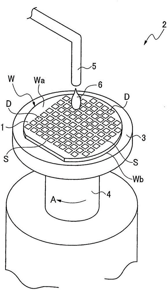
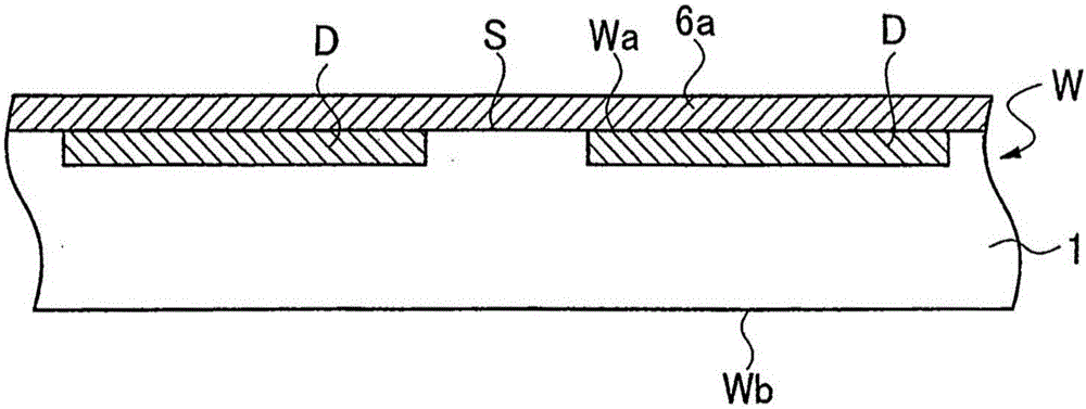
[0047] figure 1 The wafer W shown is an example of a workpiece, and includes a disc-shaped substrate 1 . A plurality of scribe lines S are formed on the front surface Wa of the wafer W, and devices D are formed in each of the areas divided by the plurality of scribe lines S. As shown in FIG. The surface on the opposite side to the front Wa constitutes the back surface Wb ground by a grinding die or the like. Next, a wafer dividing method for dividing the wafer W into individual devices D will be described.

[0048] (1) Protective film formation process

[0049] Such as figure 1 As shown, for example, a water-soluble protective film is formed on the front surface Wa of the wafer W using a spin coater 2 . The spin coater 2 has a spin table 3 that holds a wafer W and is rotatable. A rotating shaft 4 having an axis in the vertical direction is connected below the rotating table 3 . A nozzle 5 for ejecting a material liquid of a water-soluble protective film is arranged above...


PUM


Abstract

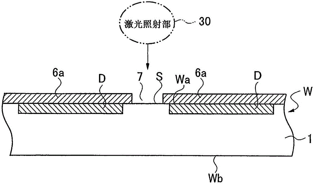
A method of dividing a wafer includes a protective film forming step of forming a water-soluble protective film on a front side of the wafer, a mask forming step of forming an etching mask on the front side of the wafer by partly removing the water-soluble protective film along the streets, a plasma etching step of performing a plasma etching on the wafer along the streets through the etching mask in the form of the water-soluble protective film, and a protective film removing step of removing the water-soluble protective film by supplying cleaning water to the water-soluble protective film. After plasma etching, i.e. in removing the protective film, the water-soluble protective film can easily be removed from the front side of the wafer simply by supplying the cleaning water from a water supply unit to the water-soluble protective film.

Description

technical field [0001] The present invention relates to a wafer dividing method for dividing a wafer into individual chips. Background technique [0002] In the manufacture of devices, a plurality of chip regions are divided by a plurality of dividing lines arranged in a grid pattern on the front surface of the wafer, and devices such as ICs and LSIs are formed in each chip region. The wafer constituted in this way is thinned to a predetermined thickness by grinding the back side, and then divided into individual chips with devices, and each chip is packaged by resin sealing, thereby being widely used in various electronic devices such as mobile phones and personal computers. . [0003] As a method of dividing a wafer, there are the following methods: a method of cutting a rotating cutting blade along a planned dividing line; , refer to the following patent literature). [0004] In addition, there is also a method of covering the front surface of the wafer with a resist f...

Claims


Application Information

Patent Timeline
Patent Type & Authority Applications(China)
IPC IPC(8): H01L21/78
CPCH01L21/78H01L21/30655H01L21/3081H01L21/31127H01L21/6836H01L2221/68327H01L2221/6834
Inventor 大浦幸伸山下阳平熊泽哲
Owner DISCO CORP
Learn More