Barrier probe provided with solid dielectric film on probe point

A dielectric and conductive probe technology, applied in the field of potential barrier probes, can solve the problems of easy falling off, inability to be applied, weak adsorption force, etc.

Pending Publication Date: 2016-11-09
HENAN NORMAL UNIV
View PDF7 Cites 3 Cited by
  • Summary
  • Abstract
  • Description
  • Claims
  • Application Information

AI Technical Summary

Problems solved by technology

Although some molecules can be classified as dielectrics, the tip modified in these ways has weak adsorption

Method used


Image

  • Barrier probe provided with solid dielectric film on probe point
  • Barrier probe provided with solid dielectric film on probe point
  • Barrier probe provided with solid dielectric film on probe point

Examples


Embodiment 1

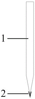
[0047] Barrier probe fabricated by depositing a solid dielectric film on the tip of a platinum-iridium alloy probe

[0048] First, cut out a sharp conductive tip from one end of a platinum-iridium alloy wire with a length of about 10 mm and a diameter of 0.15 mm with pliers or scissors to form a conductive probe 1, and then deposit a layer on the conductive tip of the conductive probe 1. A silicon dioxide solid dielectric film 2 with a thickness of about 10 nm is enough.

Embodiment 2

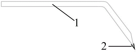
[0050] Barrier probe fabricated by depositing a solid dielectric film on a curved platinum-iridium alloy probe tip

[0051] In embodiment 1, it is sufficient to fold the platinum-iridium alloy wire into an angle of about 110° at a place about 2 mm behind the conductive tip of the conductive probe 1 . Since the probe of the scanning tunneling microscope does not need to vibrate, it is not necessary for the conductive probe to have excellent vibration stability.

Embodiment 3

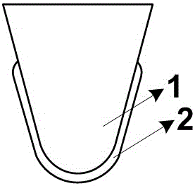
[0053] Barrier probe made by depositing solid dielectric thin film at the tip of CAFM probe

[0054] First find a probe for CAFM, and deposit a layer of silicon dioxide solid dielectric film with a thickness of about 10 nm on the conductive tip of the probe.


PUM

PropertyMeasurementUnit
Thicknessaaaaaaaaaa

Abstract

The invention discloses a barrier probe provided with a solid dielectric film on a probe point, and belongs to the probe design field of scanning probe microscopes. According to the technical schemes, the barrier probe provided with the solid dielectric film on the probe point comprises a conductive probe used for a scanning probe microscope, the conductive probe is formed by a conductive probe body and a conductive probe point arranged on a free end of the conductive probe body, and the conductive probe point is covered by at least one layer of solid dielectric film. The requirements on the hardness and chemical activity of a probe conductive material are not high, the wear resistance is good, the resolution is high, and the barrier probe is especially applicable to a scanning electrochemical microscope, a conductive atomic force microscope and a contact-mode scanning tunnel microscope and is simultaneously applicable to other scanning probe microscopes of existing modes.

Description

technical field [0001] The invention belongs to the technical field of probe design of a scanning probe microscope, in particular to a potential barrier probe with a solid dielectric thin film on a needle tip. Background technique [0002] At present, the probe materials of scanning tunneling microscopes are almost all platinum-iridium alloy materials or tungsten materials, and there are almost no other materials. The reason is that the tip of scanning probe microscope (SPM) almost always requires: (1) tip hardness as large as possible; (2) tip inertness as large as possible, especially for scanning tunneling microscope (STM). These two points limit that many materials are not suitable for SPM probes, especially STM probes. [0003] Moreover, when STM works, there needs to be an electrically insulating or nearly electrically insulating barrier material between the probe and the sample, but the insulating barrier material is not only the common gaseous state, or the liquid s...

Claims


Application Information

Patent Timeline
IPC IPC(8): G01Q60/16
CPCG01Q60/16
Inventor 李全锋李全利
Owner HENAN NORMAL UNIV
Why Eureka
Try Eureka