LTPS display panel, peripheral circuit and testing method

A technology for display panels and peripheral circuits, applied in nonlinear optics, instruments, optics, etc., can solve the problems of unfavorable narrow frame design of display panels and occupying the internal space of the frame, so as to realize narrow frame design, save peripheral space, protect The effect of the line

Active Publication Date: 2016-11-16
WUHAN CHINA STAR OPTOELECTRONICS TECH CO LTD
View PDF6 Cites 8 Cited by
  • Summary
  • Abstract
  • Description
  • Claims
  • Application Information

AI Technical Summary

Problems solved by technology

After the array substrate manufacturing process is completed, the peripheral ESD structure still exists at the end of the panel, which will occupy the internal space of the frame, which is not conducive to the narrow frame design of the display panel

Method used


Image

  • LTPS display panel, peripheral circuit and testing method
  • LTPS display panel, peripheral circuit and testing method
  • LTPS display panel, peripheral circuit and testing method

Examples


Embodiment Construction

[0035] The implementation of the present invention will be described in detail below in conjunction with the accompanying drawings and examples, so as to fully understand and implement the process of how to apply technical means to solve technical problems and achieve technical effects in the present invention. It should be noted that, as long as there is no conflict, each embodiment and each feature in each embodiment of the present invention can be combined with each other, and the formed technical solutions are all within the protection scope of the present invention.

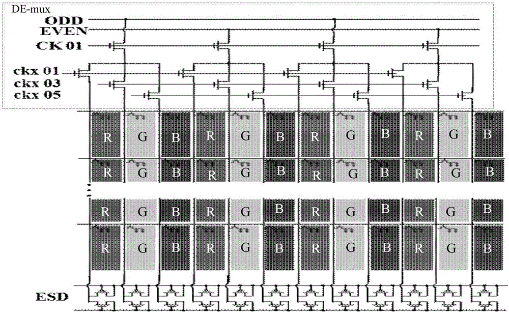
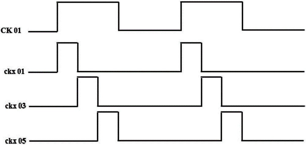
[0036] Such as figure 1 Shown is a schematic structural diagram of a traditional LTPS panel circuit in the prior art, and its peripheral circuit includes an ESD structure and a test circuit. Such as figure 1 As shown, the ESD structure is usually designed on the opposite side of the data line driving multiplexing circuit DE-mux. In the process stage of the array substrate, when the potential on the data li...


PUM


Abstract

The invention discloses an LTPS display panel, a peripheral circuit and a testing method. The peripheral circuit is characterized in that a type-N transistor and a type-P transistor are arranged at the tail end of each data line, and source and drain electrodes of the type-N transistor and the type-P transistor are correspondingly connected, wherein the correspondingly connected ends of the source and drain electrode of the type-N transistor and the type-P transistor are connected with a data line, and the other ends are connected with a signal transmission line; grid electrodes of the type-N transistor and the type-P transistor are connected with corresponding control signal lines respectively, and the signal transmission lines and the control signal lines are in short connection with ground lines. The peripheral circuit can save the space on the periphery of the panel, and the product narrow-frame design is achieved.

Description

technical field [0001] The invention belongs to the technical field of liquid crystal display control, and in particular relates to an LTPS display panel, peripheral circuits and testing methods. Background technique [0002] In order to prevent circuit damage due to excessive static electricity accumulated inside the panel, traditional LTPS (Low temperature poly-silicon, low temperature polysilicon) display panels are often provided with an electrostatic ESD protection structure. [0003] The static electricity generation process of the LTPS display panel mainly focuses on the dry etching process of the array substrate. Therefore, when designing the panel, an ESD structure is designed at the end of each data line to protect the static electricity generated during the manufacturing process of the array substrate. After the array substrate manufacturing process is completed, the peripheral ESD structure still exists at the end of the panel, which will occupy the internal spa...

Claims


Application Information

Patent Timeline
Patent Type & Authority Applications(China)
IPC IPC(8): G02F1/1362G02F1/1368
CPCG02F1/136204G02F1/136286G02F1/1368G02F1/136254
Inventor 王聪
Owner WUHAN CHINA STAR OPTOELECTRONICS TECH CO LTD
Why Eureka
Try Eureka