

Drive device
A driving device and action technology, applied in electrical components, pulse technology, electronic switches, etc., can solve problems such as insufficient switching loss effect, difficult switching timing optimization, inability to solve surge voltage and switching loss, etc.
- Summary
- Abstract
- Description
- Claims
- Application Information
AI Technical Summary
Problems solved by technology
Method used
Image

Examples
no. 1 approach
[0031] Initially, referring to figure 1 , the driving device according to this embodiment will be described.
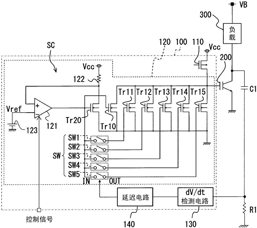
[0032] Such as figure 1 As shown, the drive device 100 controls the drive of an insulated gate bipolar transistor (IGBT) 200 serving as a power switching element that drives a load 300 .
[0033] This drive device 100 includes an on-side circuit 110 , an off-side circuit 120 , a dV / dt detection circuit, and a delay circuit 140 .
[0034] The on-side circuit 110 and the off-side circuit 120 are connected in series between a power supply and GND (ground), and the gate of the IGBT 200 is connected to an intermediate point thereof. The on-side circuit 110 is constituted by a PMOS transistor, and the power supply voltage Vcc is applied to the gate of the IGBT 200 when the PMOS transistor is in an on state. As a result, IGBT 200 is turned on, a current flows between the collector and emitter of IGBT 200 , and electric power is supplied to the load.
[0035] The off-side...
Deformed example 1
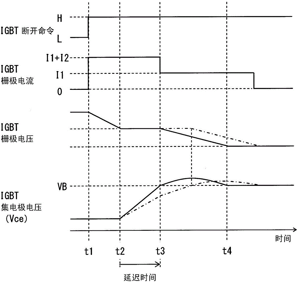
[0059] In the above-described example, an example in which the gate current of IGBT 200 is switched by turning off switching circuit SW1 from a state in which only switching circuit SW1 is turned on has been shown. In other words, an example is shown in which the number of switching stages of the gate current is two. However, it is not limited to this example. That is, the number of switching stages of the gate current may be three or more.
[0060] For example, it is also possible to Figure 5As shown in the control, switch circuits SW1 to SW3 are turned on at time t1, switch circuit SW3 is turned off at time t3, switch circuit SW2 is turned off at time t5, and switch circuit SW1 is turned off at time t6.
[0061] Accordingly, the gate current can be changed more smoothly than when the number of switching stages of the gate current is two, and thus an increase in switching loss due to the temperature characteristics of the IGBT 200 can be further suppressed.
no. 2 approach
[0063] In the above-described embodiment, an example was shown in which the control by the temperature of IGBT 200 is enabled in off-side circuit 120 , but this can also be applied to on-side circuit 110 .
[0064] Specifically, as Image 6 As shown, the pass-side circuit 110 has a plurality of PMOS transistors (Tr50-Tr55, Tr60). These PMOS transistors are composed of main MOS transistors ( Tr50 to Tr55 ) which are output transistors, and a sense MOS transistor Tr60 which regulates the drain current of the main MOS transistors. In this embodiment, six main MOS transistors ( Tr50 to Tr55 ) constitute a current mirror with respect to the sense MOS transistor Tr60 . Specifically, the gates of the main MOS transistors ( Tr50 to Tr55 ) are shared with the gate of the sense MOS transistor Tr60 , and the drains are shared with the power supply Vcc. The source of each main MOS transistor (Tr50-Tr55) is connected to the gate of IGBT200.
[0065] In addition, the on-side circuit 110 ...
PUM
 Abstract
Description
Claims
Application Information