Stress sensor, preparation method and electronic skin

A stress sensor and dielectric layer technology, applied in the field of sensors, can solve the problems of inability to measure the position of the force application point, increase the difficulty of sensor production, and low detection accuracy, and achieve the effects of simple structure, convenient operation, and high detection accuracy

Active Publication Date: 2016-11-23
BEIJING INST OF NANOENERGY & NANOSYST
View PDF5 Cites 18 Cited by
  • Summary
  • Abstract
  • Description
  • Claims
  • Application Information

AI Technical Summary

Problems solved by technology

[0002] At present, the stress sensor mainly detects external force by changing the contact area. Due to many factors affecting the contact area, the detection accuracy is not high, and it is impossible to measure information such as the position of the force application point.
In addition, stress sen

Method used


Image

  • Stress sensor, preparation method and electronic skin
  • Stress sensor, preparation method and electronic skin
  • Stress sensor, preparation method and electronic skin

Examples


preparation example Construction

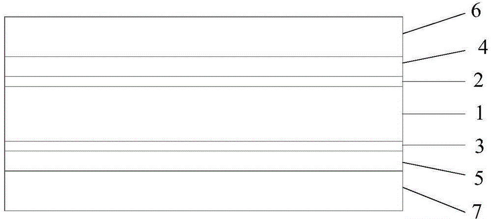
[0066] The present invention also provides a preparation method of a strain sensor, the preparation method comprising: respectively providing at least one first electrode unit and at least one second electrode unit; and coating the first electrode unit and the second electrode unit Cover a thin film to form a dielectric layer, so that the first electrode unit is arranged on the upper surface of the dielectric layer, the second electrode unit is arranged on the lower surface of the dielectric layer, and the second The electrode unit crosses the first electrode unit to form a capacitor array.

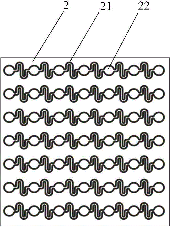
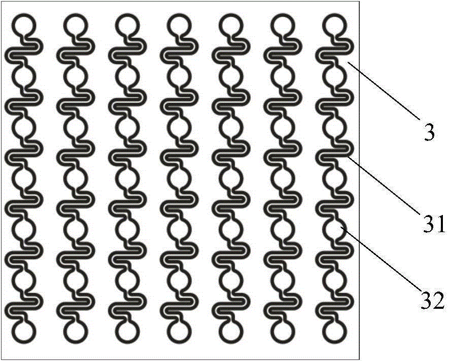
[0067] Wherein, the first electrode unit includes a curved first wire, and a first conductive node is provided on the first wire; the second electrode unit includes a curved second wire, and the second wire is provided with a A second conductive node is provided; the first conductive node and the second conductive node are respectively the upper plate or the lower plate of the correspondi...


PUM

PropertyMeasurementUnit
Widthaaaaaaaaaa
Thicknessaaaaaaaaaa
Thicknessaaaaaaaaaa

Abstract

The invention relates to the field of sensor technology, and discloses a stress sensor, a preparation method and an electronic skin. The stress sensor includes: a dielectric layer (1), used for elastic deformation under the action of an external force; at least one first electrode unit ( 2), having stretchability, disposed on the upper surface of the dielectric layer (1); and at least one second electrode unit (3), having stretchability, disposed on the dielectric layer (1) The lower surface of the first electrode unit (2) and the second electrode unit (3) cross relatively to form a capacitor array; under the action of an external force, the vertical distance of the corresponding relative intersection changes, so that the capacitance on the corresponding capacitor Variety. The stress sensor of the invention can accurately detect the variation of capacitance and has high detection precision.

Description

technical field [0001] The invention relates to the technical field of sensors, in particular to a stress sensor, a preparation method and an electronic skin. Background technique [0002] At present, stress sensors mainly detect external forces by changing the contact area. Due to many factors affecting the contact area, the detection accuracy is not high, and it is impossible to measure information such as the position of the force application point. In addition, stress sensors are mainly made of special materials such as graphene and carbon nanotubes with excellent properties such as ultra-thin, stretchable, and low resistivity. However, the synthesis of these cutting-edge materials increases the difficulty of sensor production, and the yield rate Low, high production cost. Contents of the invention [0003] The object of the present invention is to provide a stress sensor that can accurately detect the variation of capacitance. [0004] In order to achieve the above ...

Claims


Application Information

Patent Timeline
IPC IPC(8): G01L1/14G01L9/12
Inventor 潘曹峰赵晓丽
Owner BEIJING INST OF NANOENERGY & NANOSYST
Why Eureka
Try Eureka