
Wafer support ring, wafer support jig and wafer processing equipment

A technology for wafer processing and support rings, which is applied in the manufacture of electrical components, circuits, semiconductors/solid-state devices, etc. It can solve problems such as the inability to ensure consistent wafer temperature, lower chip yield, and cumbersome adjustment process, and achieve simple structure and easy operation , the effect of large contact area

Active Publication Date: 2019-01-11
48TH RES INST OF CHINA ELECTRONICS TECH GROUP CORP
View PDF4 Cites 0 Cited by
  • Summary
  • Abstract
  • Description
  • Claims
  • Application Information

AI Technical Summary

Problems solved by technology

This positioning method needs to adjust the tops of each thimble to the same height. The adjustment process is very cumbersome and the accuracy cannot be guaranteed. It is also difficult to keep at the same height during use; It is easy to cause debris during the process; in addition, the area supported by the thimble is generally in the area where the chip is made on the wafer. When the process needs to heat the wafer, the thimble will affect the temperature of the wafer surface, and it is impossible to ensure that the temperature of each area of ​​the wafer is consistent. The yield rate of the chip is reduced

Method used


Image

  • Wafer support ring, wafer support jig and wafer processing equipment
  • Wafer support ring, wafer support jig and wafer processing equipment
  • Wafer support ring, wafer support jig and wafer processing equipment

Examples


Embodiment 1

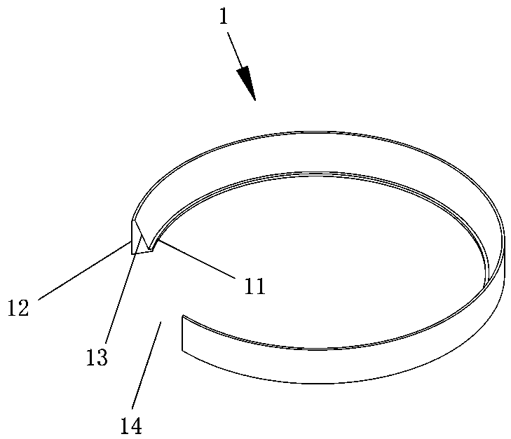
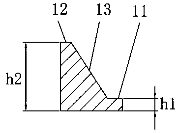
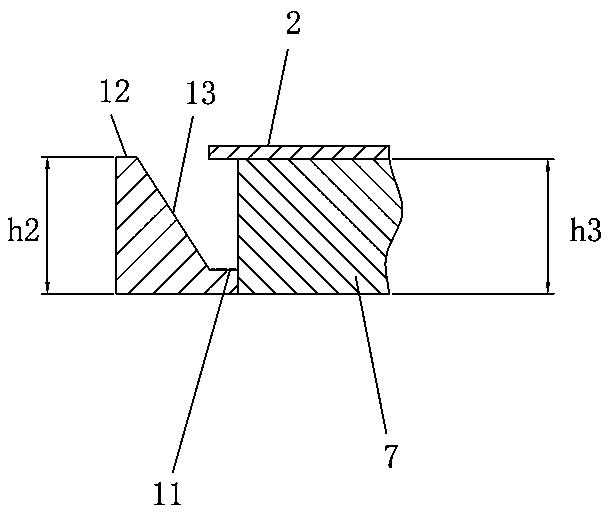
[0027] Such as Figure 1 to Figure 3 As shown, the wafer support ring of the present embodiment includes a support ring body 1, and the support ring body 1 includes an outer ring portion 12 and an inner ring portion 11 for supporting the wafer 2, the height of the inner ring portion 11 is h1, and the outer ring portion The height of 12 is h2, h1<h2, the outer side of the upper surface of the inner ring part 11 and the inner side of the upper surface of the outer ring part 12 are transitionally connected by a slope 13, the wafer support ring is provided with an inner ring part 11 for placing the wafer 2, and the inner ring part The flatness of the part 11 can be guaranteed by the machining accuracy, so as to ensure the accurate positioning of the wafer 2, without complicated adjustments, and easy to use. The inner ring part 11 can provide effective support for the outer peripheral part of the wafer 2, and the contact area is larger and the force is more uniform , reducing fragm...

Embodiment 2

[0030] Such as Figure 4 with Figure 5 As shown, the wafer support ring of this embodiment is basically the same as that of Embodiment 1, the difference is that the height difference between the inner ring portion 11 and the outer ring portion 12 is relatively small, and accordingly, the specification of the inclined surface 13 is also reduced. The processing difficulty of the wafer support ring is reduced.

[0031] Such as Image 6 As shown, the wafer supporting fixture of this embodiment includes a reinforcing ring 4, a connecting rod 5 and the above-mentioned wafer supporting ring, the reinforcing ring 4 is located below the supporting ring body 1, the upper end of the connecting rod 5 is fixedly connected to the supporting ring body 1, and the connecting rod 5. The lower end is fixedly connected with the reinforcement ring 4. The wafer support fixture includes the above-mentioned wafer support ring, so it also has the advantages of the wafer support ring, and has a simp...


PUM


Abstract

A wafer supporting ring comprises a supporting ring body, the supporting ring body comprises an outer ring part and an inner ring part, the height of the inner ring part is smaller than that of the outer ring part, and the outer side of the upper surface of the inner ring part and the inner side of the upper surface of the outer ring part are in transition connection through a slope. A wafer supporting clamp comprises a reinforcing ring, connecting rods and the wafer supporting ring, the reinforcing ring is located below the supporting ring body, the upper ends of the connecting rods are fixedly connected with the supporting ring body, and the lower ends of the connecting rods are fixedly connected with the reinforcing ring. Wafer processing equipment comprises a heating plate, a wafer carrying plate is arranged on the upper surface of the heating plate, the wafer processing equipment further comprises the wafer supporting clamp and a driving device used for driving the wafer supporting clamp to move vertically, the supporting ring body is located above the wafer carrying plate, the reinforcing ring is located below the heating plate, the driving device is connected with the reinforcing ring, the connecting rods penetrate through the heating plate, and the height of the wafer carrying plate is not smaller than that of the inner ring part. The wafer supporting ring has the advantages of being simple in structure, convenient to use, uniform in stress, good in supporting stability and the like.

Description

technical field [0001] The invention relates to equipment for manufacturing semiconductors, in particular to a wafer support ring, a wafer support fixture and wafer processing equipment. Background technique [0002] The integrated circuit and semiconductor manufacturing industries promote the realization of equipment automation. The function of some semiconductor equipment is to process the wafer through physical and chemical means. This process is called semiconductor process. Most of the semiconductor process is in a vacuum sealed reaction chamber. Therefore, it is necessary to accurately transfer the wafer to be processed into the reaction chamber and position it accurately. [0003] At present, most of the semiconductor processes use manipulators to transfer wafers or trays into the reaction chamber, and then remove the wafers or trays from the reaction chamber after processing. The pick-and-place process is usually achieved by the cooperation of manipulators and thimbl...

Claims


Application Information

Patent Timeline
Patent Type & Authority Patents(China)
IPC IPC(8): H01L21/687H01L21/67
CPCH01L21/67098H01L21/68735H01L21/68785
Inventor 罗才旺肖慧罗臻
Owner 48TH RES INST OF CHINA ELECTRONICS TECH GROUP CORP
Learn More