Inverse LED chip and manufacturing method thereof

A technology of LED chip and manufacturing method, which is applied in the direction of electrical components, circuits, semiconductor devices, etc., can solve the problems of packaging yield loss, difficult soldering, and light efficiency per unit area to be improved, so as to improve simplicity and improve packaging yield Effect

Inactive Publication Date: 2016-11-23
ENRAYTEK OPTOELECTRONICS
View PDF9 Cites 3 Cited by
  • Summary
  • Abstract
  • Description
  • Claims
  • Application Information

AI Technical Summary

Problems solved by technology

[0007] However, the P and N electrodes of the existing flip chip are usually on the same side of the LED chip, which requires relatively high packaging tec...

Method used


Image

  • Inverse LED chip and manufacturing method thereof
  • Inverse LED chip and manufacturing method thereof
  • Inverse LED chip and manufacturing method thereof

Examples


Embodiment Construction

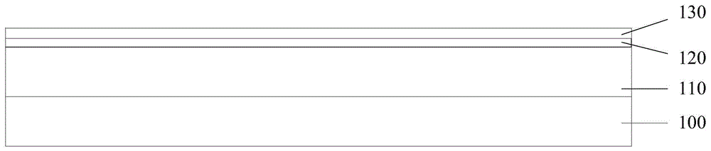
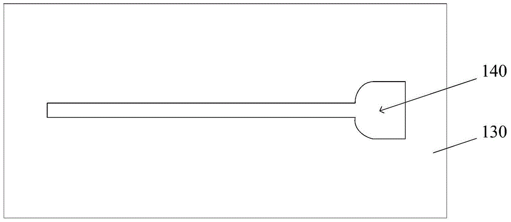
[0045] It can be seen from the background technology that the P and N electrodes of the existing flip-chip LED chip structure are usually on the same side of the chip, so the requirements for packaging technology are relatively high, which may easily cause the loss of packaging yield.

[0046] Although there are a few companies whose flip-chip product designs can realize the distribution of P and N electrodes on both sides of the chip, their designs use the method of connecting the N electrodes to the substrate through through holes, resulting in low packaging yield. In addition, the light output area lost by the LED chip is relatively large, and the area of ​​the high-reflection mirror surface is small, resulting in a decrease in light efficiency per unit area. Therefore, the packaging yield of existing flip-chip LED chips is low, and there is still room for improvement in light efficiency per unit area.

[0047] Therefore, the present invention provides a new flip-chip LED c...


PUM


Abstract

The invention relates to an inverse LED chip and a manufacturing method thereof. The method comprises steps that an epitaxial lamination layer is deposited on a substrate, and the epitaxial lamination layer comprises a first semiconductor layer, a quantum well layer and a second semiconductor layer; the epitaxial lamination layer is etched till a groove of which a bottom portion exposes the first semiconductor layer is formed, and a residual part of the epitaxial lamination layer is a Mesa platform; a first electrode is deposited on the first semiconductor layer at the bottom portion of the groove, and a gap is formed between the first electrode and the Mesa platform; an insulation layer which covers the first electrode and completely fills the gap is formed; an electrode expansion layer is formed on the Mesa platform and the insulation layer; the electrode expansion layer is connected with a conductive substrate; the substrate and the epitaxial lamination layer are separated to expose a light emitting surface of the first semiconductor layer; the light emitting surface of the first semiconductor layer is etched till a part of the first electrode is exposed. The method is advantaged in that the yield of inverse LED chips is improved.

Description

technical field [0001] The invention relates to the field of LED manufacturing, in particular to a flip-chip LED chip and a manufacturing method thereof. Background technique [0002] A light emitting diode (Light Emitting Diode, LED) chip, also called an LED (light emitting) chip, is a solid-state semiconductor device. The light-emitting diode in the LED chip uses a semiconductor PN junction as a light-emitting material, which can convert electricity into light. When emitting light, a forward voltage is applied to both ends of the semiconductor PN junction, and the electrons and holes injected into the PN junction recombine, and the excess energy is released in the form of photons. The wavelength of light is the color of light, which is determined by the material forming the PN junction. [0003] LED chips have photoelectric performance characteristics such as low energy consumption, small size, long life, good stability, fast response and stable luminous wavelength, and ...

Claims


Application Information

Patent Timeline
IPC IPC(8): H01L33/00H01L33/14H01L33/10H01L33/38
CPCH01L33/007H01L33/10H01L33/14H01L33/385H01L2933/0016
Inventor 徐慧文张宇李起鸣
Owner ENRAYTEK OPTOELECTRONICS
Why Eureka
Try Eureka