Display panel and electronic equipment

A technology for display panels and electronic equipment, applied in the fields of electrical digital data processing, optics, instruments, etc., can solve the problems of low capacitance change, low signal-to-noise ratio, and low sensitivity, so as to improve signal-to-noise ratio, reduce power consumption, Effect of Improving Detection Sensitivity

Active Publication Date: 2016-12-07
SHANGHAI CHUANGGONG COMM TECH
View PDF12 Cites 1 Cited by
  • Summary
  • Abstract
  • Description
  • Claims
  • Application Information

AI Technical Summary

Problems solved by technology

[0004] 1. Due to the separate existence of each TP board circuit, it is connected to the driver chip through 2-3 metal wires, such as image 3 As shown (31 in the figure is the touch sensor, 32 is the wiring of the touch sensor), each TP board has a square capacitive electrode plate with a length of about 4.5mm, so the load is very large, which leads to large power consumption
The main factor affecting its load is the coupling effect of capacitance, because if the shielding layer is used on the side of the backlight module 6, it will also lead to the introduction of coupling load between the TP board and the shielding layer
[0005] 2. When there is a shielding layer or a metal coupling layer under the TP sensor, the TP board will charge the coupling capacitance between the shielding layer or the metal coupling layer and the TP board, and will also charge the coupling capacitance between the hand and the TP board when there is a hand. The coupling capacitor is charged, and the capacitance of the TP sensor changes as Figure 4 As shown (1 in the figure is the glass cover, 2 is the touch sensor, 3 is the color filter, 5 is the thin film transistor, 6 is the backlight module, 7 is the shielding layer, 8 is the gap between the finger and the touch sensor Coupling capacitance, 9 is the coupling capacitance between the TP sensor and the shielding layer), because the TP sensor has the following conductive layer (shielding layer or metal coupling layer), the capacitance change sensed by the TP sensor is relatively low, and the sensitivity is low. low signal to noise ratio

Method used


Image

  • Display panel and electronic equipment
  • Display panel and electronic equipment
  • Display panel and electronic equipment

Examples


Embodiment Construction

[0019] In order to make the object, technical solution and advantages of the present invention clearer, various embodiments of the present invention will be described in detail below in conjunction with the accompanying drawings. However, those of ordinary skill in the art can understand that, in each implementation manner of the present invention, many technical details are provided for readers to better understand the present application. However, even without these technical details and various changes and modifications based on the following implementation modes, the technical solution claimed in this application can also be realized.

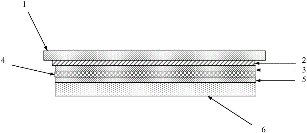
[0020] The first embodiment of the present invention relates to a display panel, such as Figure 5 As shown, it includes: TP In-Cell liquid crystal display module 4, resonant layer 10 and shielding layer 7 (1 in the figure is a glass cover plate, 2 is a touch sensor, 3 is a color filter, 4 is a liquid crystal display module, 5 is a thin fi...


PUM

PropertyMeasurementUnit
lengthaaaaaaaaaa

Abstract

The invention relates to the electronic technology field and discloses a display panel and electronic equipment. The display panel comprises a TP IN-Cel liquid crystal display module, a resonance layer and a shielding layer. The resonance layer is located between the TP IN-Cel liquid crystal display module and the shielding layer. The resonance layer is located on the backlight side of the TP IN-Cel liquid crystal display module. In the display time slot, the resonance layer keeps first constant voltage. In the touch control scanning time slot, a touch control sensor and a public electrode both receive scanning signals and are used for charging and discharging electricity of the touch control sensor. The resonance layer is used for receiving pre-set voltage signals. The pre-set voltage signals and the scanning signals are the same in terms of phase and amplitude. The embodiment of the invention further provides the electronic equipment. Compared with the prior art, the embodiment has following beneficial effects: coupling load between a TP plate and the shielding layer can be reduced and power consumption is reduced; energy utilization rate is increased; capacitance change amount sensed by a TP sensor is increased; and detection flexibility is improved.

Description

technical field [0001] The invention relates to the technical field of display panels, in particular to a display panel and electronic equipment. Background technique [0002] In the prior art, the stacked structure of the TP In-Cell (touch sensor embedded in the display) display panel is as follows: figure 1 As shown (in the figure 1 is the glass cover, 2 is the touch sensor, 3 is the color filter, 4 is the liquid crystal display module, 5 is the thin film transistor, 6 is the backlight module), wherein the touch sensor is located on the glass Between the cover plate and the backlight module 6 , the touch sensor generally adopts a self-capacitive touch solution, also known as Full In-Cell and TDDI In-Cell. Its technical feature is that the touch sensor in the panel and the common electrode (Vcom) in the display circuit share conductive lines and electrodes. [0003] The TP In-Cell display panel adopts the drive method of time-sharing scanning, and the scanning sequence di...

Claims


Application Information

Patent Timeline
Patent Type & Authority Applications(China)
IPC IPC(8): G06F3/044G02F1/1333
CPCG02F1/13338G06F3/044
Inventor 孙云刚
Owner SHANGHAI CHUANGGONG COMM TECH
Why Eureka
Try Eureka