Top-emission organic light emitting diode (OLED) structure and fabrication method thereof

A manufacturing method and top-emission technology, applied in semiconductor/solid-state device manufacturing, organic semiconductor devices, electrical components, etc., can solve problems such as light loss and poor OLED luminous efficiency, and achieve the effect of improving luminous efficiency

Inactive Publication Date: 2016-12-07
TCL CHINA STAR OPTOELECTRONICS TECH CO LTD
View PDF6 Cites 2 Cited by
  • Summary
  • Abstract
  • Description
  • Claims
  • Application Information

AI Technical Summary

Problems solved by technology

However, in the process of emitting light generated by the light-emitting layer to the air, there will be a large amount of light loss, so that the light-emitting efficiency of the OLED is not good.

Method used


Image

  • Top-emission organic light emitting diode (OLED) structure and fabrication method thereof
  • Top-emission organic light emitting diode (OLED) structure and fabrication method thereof
  • Top-emission organic light emitting diode (OLED) structure and fabrication method thereof

Examples


Embodiment Construction

[0020] Hereinafter, embodiments of the present invention will be described in detail with reference to the accompanying drawings. This invention may, however, be embodied in many different forms and should not be construed as limited to the specific embodiments set forth herein. Rather, the embodiments are provided to explain the principles of the invention and its practical application, thereby enabling others skilled in the art to understand the invention for various embodiments and with various modifications as are suited to particular intended uses.

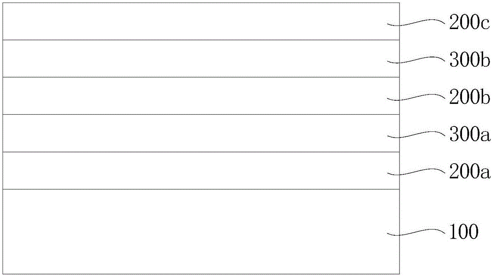
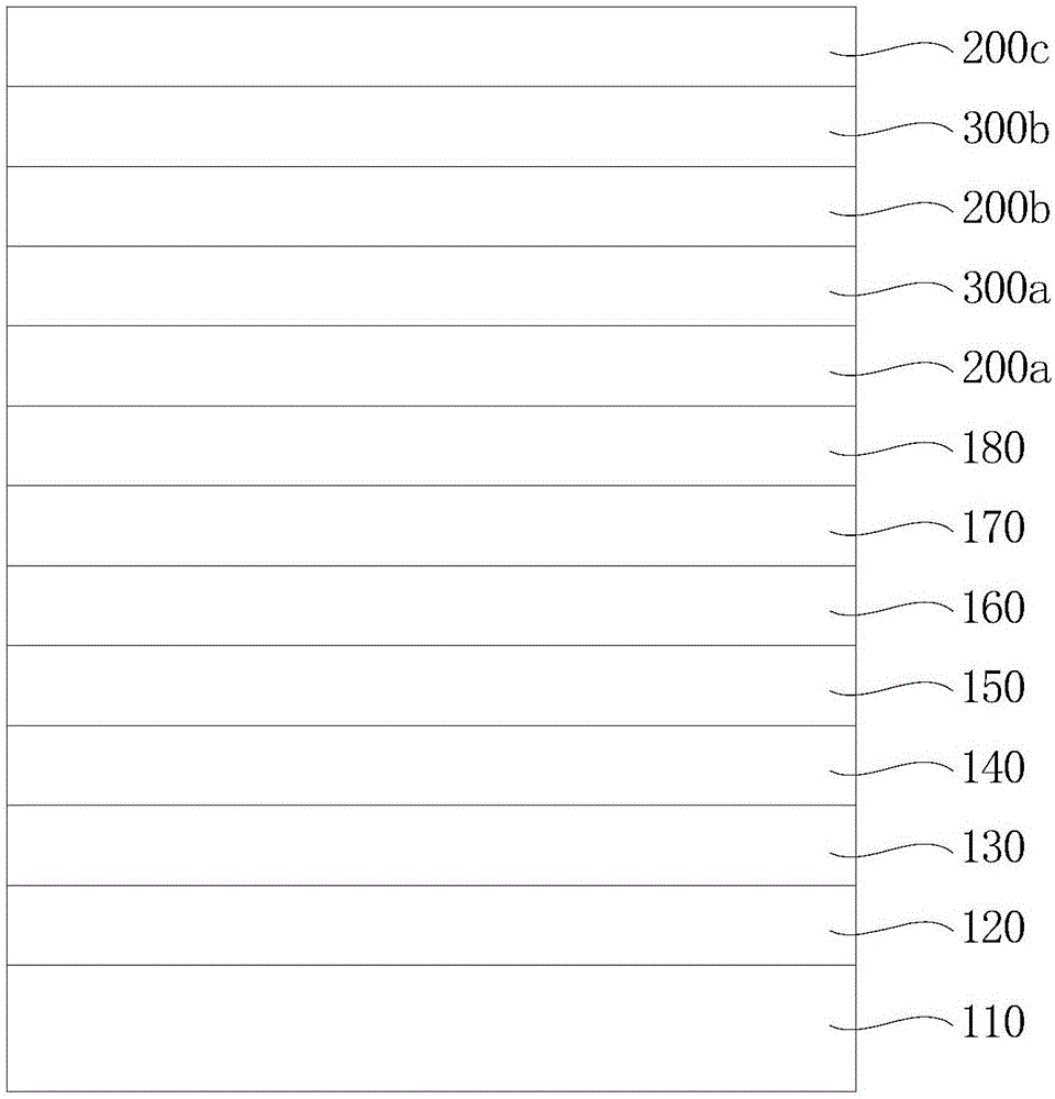
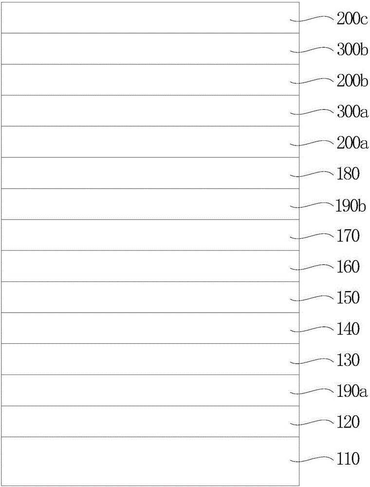
[0021] In the drawings, the thicknesses of layers and regions are exaggerated for device clarity. Like reference numerals refer to like elements throughout the drawings.

[0022] It will be understood that, although the terms "first", "second", etc. may be used herein to describe various elements, these elements should not be limited by these terms. These terms are only used to distinguish one element from another.

[0023...


PUM

PropertyMeasurementUnit
Glass transition temperatureaaaaaaaaaa

Abstract

The invention discloses a top-emission organic light emitting diode (OLED) structure. The top-emission OLED structure comprises an OLED, a plurality of blocking layers and buffer layers, wherein the buffer layers are arranged between each two adjacent blocking layers, each blocking layer has the capability of moisture oxygen blocking, and at least one buffer layer has the capability of scattering light beam. The invention also discloses a fabrication method of the top-emission OLED structure. Since the buffer layers have the capability of scattering light beam, more light can be irradiated to air, and thus, the luminous efficiency of a device is improved.

Description

technical field [0001] The invention belongs to the technical field of organic light-emitting displays, and in particular relates to a top-emitting OLED structure and a manufacturing method thereof. Background technique [0002] In the current field of lighting and display technology, organic light-emitting diodes (OLEDs) have been widely studied due to their characteristics such as low starting voltage, thinness, and self-illumination, so as to meet the needs of low energy consumption, thinness, and surface light source. [0003] The luminescence of OLED is mainly through the recombination of excitons, and then exits from the light-emitting layer into the air. However, when the light generated by the light-emitting layer is emitted to the air, a large amount of light is lost, so that the light-emitting efficiency of the OLED is not good. Therefore, how to improve the luminous efficiency of OLED is a technical problem that needs to be solved urgently. Contents of the inve...

Claims


Application Information

Patent Timeline
IPC IPC(8): H01L51/52H01L51/56
CPCH10K50/8445H10K50/854H10K50/19H10K2102/3026H10K71/00
Inventor 黄辉
Owner TCL CHINA STAR OPTOELECTRONICS TECH CO LTD
Why Eureka
Try Eureka