Laser processing method for LED wafer

A laser processing method and processing method technology, applied in the direction of laser welding equipment, metal processing equipment, manufacturing tools, etc., can solve the problems of low electrical yield rate, achieve the effect of improving yield rate, wide application space, and reducing peak power

Inactive Publication Date: 2016-12-21
HANS LASER TECH IND GRP CO LTD
View PDF5 Cites 13 Cited by
  • Summary
  • Abstract
  • Description
  • Claims
  • Application Information

AI Technical Summary

Problems solved by technology

[0008] The purpose of the embodiments of the present invention is to provide a laser processing method for LED wafers, which ...

Method used


Image

  • Laser processing method for LED wafer
  • Laser processing method for LED wafer
  • Laser processing method for LED wafer

Examples


Embodiment Construction

[0025] The present invention will be further described below with reference to the accompanying drawings and embodiments.

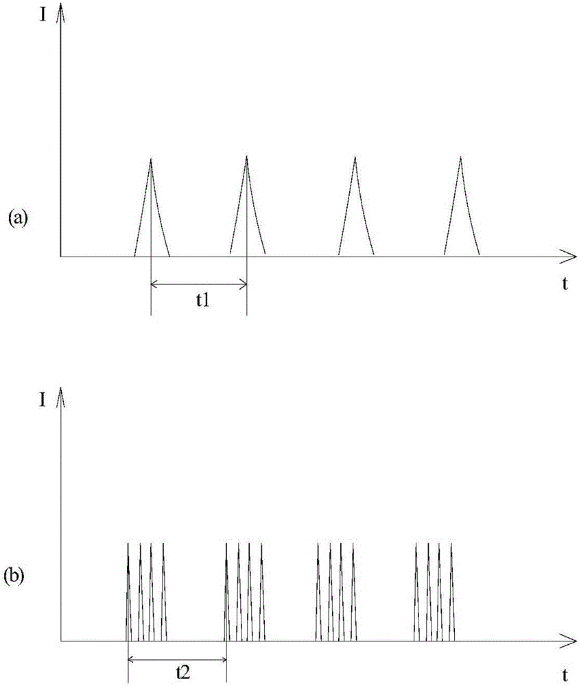
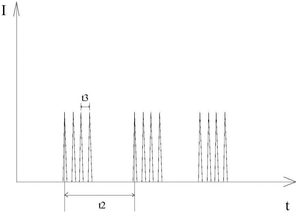
[0026] figure 1 Shown is the comparative schematic diagram of the pulse output of the existing laser and the present invention, such as figure 1 (a) shows the output mode of the existing pulsed laser, and there are single pulse outputs arranged periodically on the time axis t, each pulse has a certain intensity I, and the time interval t1 between adjacent output pulses is a fixed value , and t1=1 / laser output frequency, for example, if the laser output frequency is 50kHz, t1=1 / 50kHz=20us. figure 1 (b) shows that the implementation of the present invention provides a laser processing method, the processing method uses a pulsed laser, and the pulsed laser outputs the laser in a burst mode, or a burst sub-pulse mode, or a burst mode (burst mode) pulse output mode , where the burst sub-pulse mode and the burst mode (burst mode) pulse output mode are coordin...


PUM


Abstract

The invention provides a laser processing method for an LED wafer. According to the processing method, by adopting a pulse laser, the pulse laser outputs lasers in form of pulse trains or pulse envelopes. Each of the pulse trains or pulse envelopes comprises a plurality of sub pulses, and the time interval of each of the pulse trains or pulse envelopes is fixed. According to the laser processing method, the focuses formed on the LED wafer are round. The pulse trains or pulse envelopes on the laser cut LED wafer output lasers, so that the peak power of lasers for cutting the LED wafer is effectively reduced, the influence of the lasers on an LED wafer light-emitting region is reduced, and the electrical parameter yield of the LED wafer is improved, for example, forward voltage Vf, reverse current Ir, brightness and the like. The laser processing method for the LED wafer provided by the embodiment of the invention has a wide application space in the LED wafer laser cutting industry.

Description

technical field [0001] The invention belongs to the field of laser processing, in particular to a laser processing method of an LED wafer. Background technique [0002] In the semiconductor industry such as LED wafers using laser micro-precision processing, sapphire is generally used as the substrate material, and the light-emitting area is deposited on the sapphire substrate. The thickness of the light-emitting area is generally only 3 to 6um, and the thickness of sapphire is generally 80-150um. . At present, lasers are generally used to process LED wafers to separate them into individual small chips. Laser processing is generally incident from the sapphire surface of the wafer to a certain depth. For LED wafers with a certain thickness, the parameters of laser processing have a direct impact on the quality of processing. [0003] Laser processing parameters include laser parameters, such as pulse width, wavelength, polarization state, peak power, etc.; in addition, laser...

Claims


Application Information

Patent Timeline
IPC IPC(8): B23K26/0622B23K26/38B23K26/402
CPCB23K26/0622B23K26/38B23K26/402
Inventor 王焱华庄昌辉马国东曾威朱炜尹建刚高云峰
Owner HANS LASER TECH IND GRP CO LTD
Why Eureka
Try Eureka