Pixel structure and liquid crystal display panel

A liquid crystal display panel and pixel structure technology, applied in nonlinear optics, instruments, optics, etc., can solve the problems of low aperture ratio and complex structure, achieve low aperture ratio, solve the problem of color shift, and improve the effect of aperture ratio

Active Publication Date: 2016-12-21
TCL CHINA STAR OPTOELECTRONICS TECH CO LTD
View PDF5 Cites 22 Cited by
  • Summary
  • Abstract
  • Description
  • Claims
  • Application Information

AI Technical Summary

Problems solved by technology

[0005] The purpose of the present invention is to provide a pixel structure to solve the technical problems in the existing pixel structure

Method used


Image

  • Pixel structure and liquid crystal display panel
  • Pixel structure and liquid crystal display panel
  • Pixel structure and liquid crystal display panel

Examples


Embodiment Construction

[0032] In order to further illustrate the technical means adopted by the present invention and its effects, the following describes in detail in conjunction with preferred embodiments of the present invention and accompanying drawings.

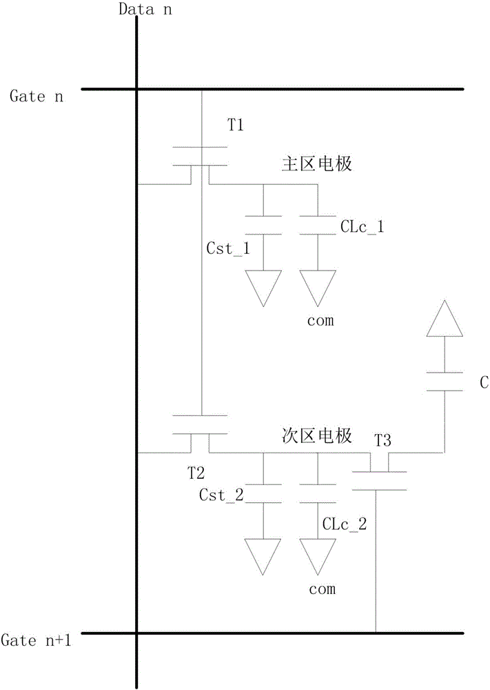
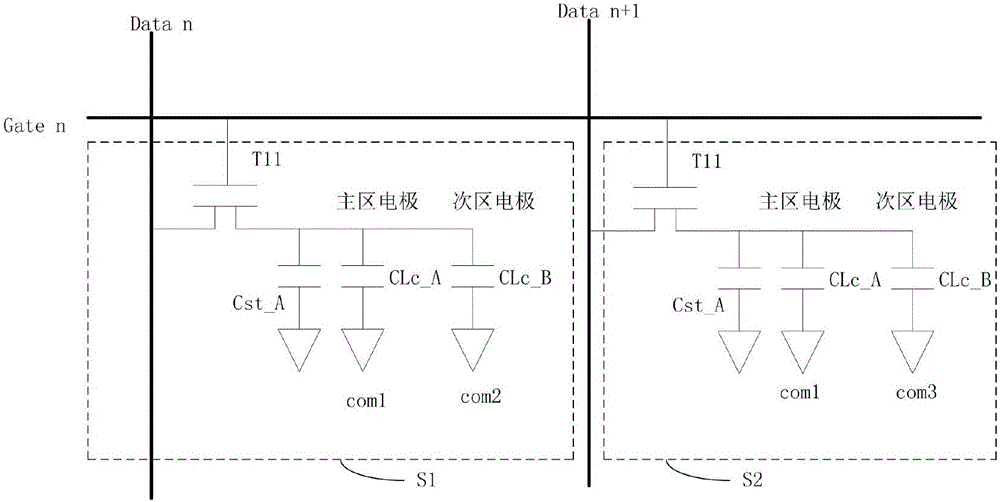
[0033] The pixel structure of the present invention includes: a common electrode, which includes a first common electrode and a second common electrode group; a plurality of pixel units formed by intersections of a plurality of scanning lines and data lines, and each of the pixel units corresponds to one of the A scan line and a data line, and include a main area electrode, a sub area electrode and a thin film transistor; wherein, the gate of the thin film transistor is connected to the scan line corresponding to the pixel unit, and the source is connected to the data corresponding to the pixel unit Lines and drains are respectively connected to the main area electrode and the sub area electrode; the main area electrode corresponds to the first...


PUM


Abstract

The invention provides a pixel structure and a liquid crystal display panel. The pixel structure comprises a first public electrode and a second public electrode set, wherein a plurality of scanning lines and data lines are crossed and formed into a plurality of pixel units; each pixel unit is corresponding to each scanning line and each data line and comprises a main area electrode, a secondary area electrode and a thin film transistor; a grid electrode of the thin film transistor is connected with the scanning line corresponding to the pixel unit, a source electrode is connected with the data line corresponding to the pixel unit and a drain electrode is respectively connected with a main area electrode and a secondary area electrode; the main area electrode is corresponding to the first public electrode; the secondary area electrode is corresponding to the second public electrode set; different voltages are applied to the first public electrode and the second public electrode set, so that the liquid crystals in the pixel areas corresponding to the main area electrode and the secondary area electrode are deflected for different degrees. According to the pixel structure and the liquid crystal display panel provided by the invention, the structure is simple, the opening rate is increased and the color cast phenomenon is avoided.

Description

technical field [0001] The invention relates to the field of liquid crystal display panels, in particular to a pixel structure and a liquid crystal display panel. Background technique [0002] The existing VA (Vertical Alignment, vertical alignment) liquid crystal display panel has become a mainstream product in the market due to its advantages such as wide viewing angle and high contrast ratio. VA-type liquid crystal display panels generally have color shift problems, such as figure 1 Shown is a schematic diagram of an equivalent circuit of a pixel unit of an existing liquid crystal display panel using charge sharing technology. By dividing the pixel electrode of each pixel unit into two parts, the main area electrode and the sub area electrode, the main area electrode is driven by the thin film transistor T1, and the sub area electrode is driven by the thin film transistors T2, T3 and a shared capacitor C. Specifically, the liquid crystal display panel performs progressi...

Claims


Application Information

Patent Timeline
IPC IPC(8): G02F1/1362G02F1/1368G02F1/1343
CPCG02F1/134309G02F1/136227G02F1/136286G02F1/1368
Inventor 张蒙蒙岳守振
Owner TCL CHINA STAR OPTOELECTRONICS TECH CO LTD
Why Eureka
Try Eureka